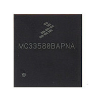
MC33580BAPNA Freescale, MC33580BAPNA Datasheet - Page 18

MC33580BAPNA
Manufacturer Part Number
MC33580BAPNA
Description
Manufacturer
Freescale
Datasheet
1.MC33580BAPNA.pdf
(38 pages)
Specifications of MC33580BAPNA
Switch Type
High Side
Power Switch Family
MC33580
Input Voltage
6 to 27V
Power Switch On Resistance
30mOhm
Number Of Outputs
4
Mounting
Surface Mount
Supply Current
20mA
Package Type
Power QFN
Operating Temperature (min)
-40C
Operating Temperature Classification
Automotive
Pin Count
24
Lead Free Status / RoHS Status
Compliant
Available stocks
Company
Part Number
Manufacturer
Quantity
Price
SPI PROTOCOL DESCRIPTION
synchronous data transfer with four I/O lines associated with
it: Serial Input (SI), Serial Output (SO), Serial Clock (SCLK),
and Chip Select (
Fault, and Fail-Safe.
succeeding paragraphs.
18
33580
Table 5. Fail-Safe Operation and Transitions to Other
FUNCTIONAL DEVICE OPERATION
OPERATIONAL MODES
Normal
x = Don’t care.
Mode
Sleep
Fault
Safe
Fail-
The SPI interface has a full duplex, three-wire
The 33580 has four operating modes: Sleep, Normal,
33580 Modes
FS
CSB
SCLK
CS
x
1
0
0
0
1
1
1
SO
SI
NOTES:
Notes
Wake RST WDTO
0
x
1
1
0
0
1
1
CS
D15
1.
2.
OD15
).
Table 5
1.
2. D15
3. OD15
RSTB is in a logic H state during the above operation.
DO, D1, D2, ... , and D15 relate to the most recent ordered entry of program data into the LUX IC
0
1
1
0
1
1
1
0
RST
D14
OD14
:
summarizes details contained in
Yes
is a logic [1] state during the above operation.
No
No
D0 relate to the most recent ordered entry of data into the device.
x
:
OD0 relate to the first 16 bits of ordered fault and status data out of the device.
D13
OD13
Device is in Sleep mode. All
outputs are OFF
Normal mode. Watchdog is
active if enabled.
Device is currently in fault
mode. The faulted output(s)
is (are) OFF.
Watchdog has timed out and
the device is in Fail-Safe
Mode. The outputs are as
configured with the RFS
resistor connected to FSI.
RST
from logic [1] to logic [0]
simultaneously to bring the
device out of the Fail-safe
mode or momentarily tied the
FSI pin to ground.
D12
OD12
Figure 9. Single 16-Bit Word SPI Communication
FUNCTIONAL DEVICE OPERATION
and WAKE must go
Comments
D11
OD11
CS
D10
OD10
OPERATIONAL MODES
D9
OD9
D8
OD8
to D0) protocol, with both input and output words transferring
the most significant bit (MSB) first. All inputs are compatible
with 5.0 V CMOS logic levels.
SLEEP MODE
the state of the device after first applying battery voltage
(V
device when the WAKE and
Sleep mode, the output and all unused internal circuitry, such
as the internal 5.0 V regulator, are off to minimize current
draw. In addition, all SPI-configurable features of the device
are as if set to logic [0]. The 33580 will transition to the
Normal or Fail-Safe operating modes based on the WAKE
and
NORMAL MODE
FAIL-SAFE MODE
Fail-Safe Mode and Watchdog
detection is active when either the WAKE or
transitions from logic [0] to logic [1]. The WAKE input is
capable of being pulled up to V
D7
OD7
PWR
The SI / SO pins of the 33580 follow a first-in first-out (D15
The Default mode of the 33580 is the Sleep mode. This is
The 33580 is in Normal mode when:
• V
•
• No fault has occurred.
If the FSI input is not grounded, the watchdog timeout
RST
RST
D6
) prior to any I/O transitions. This is also the state of the
PWR
OD6
inputs as defined in
pin is logic [1].
and V
D5
OD5
DD
D4
OD4
are within the normal voltage range.
device.
Analog Integrated Circuit Device Data
D3
OD3
RST
Table
D2
OD2
PWR
are both logic [0]. In the
Freescale Semiconductor
5.
with a series of limiting
D1
OD1
D0
OD0
RST
input pin


