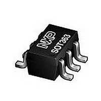
74AUP1T97GW NXP Semiconductors, 74AUP1T97GW Datasheet - Page 11

74AUP1T97GW
Manufacturer Part Number
74AUP1T97GW
Description
Manufacturer
NXP Semiconductors
Datasheet
1.74AUP1T97GW.pdf
(20 pages)
Specifications of 74AUP1T97GW
Logic Family
AUP
Technology
CMOS
High Level Output Current
-4mA
Low Level Output Current
4mA
Operating Supply Voltage (typ)
2.5/3.3V
Package Type
SOT-363
Operating Supply Voltage (max)
3.6V
Operating Supply Voltage (min)
2.3V
Abs. Propagation Delay Time
11.9ns
Mounting
Surface Mount
Pin Count
6
Operating Temperature (min)
-40C
Operating Temperature (max)
125C
Operating Temperature Classification
Automotive
Lead Free Status / RoHS Status
Compliant
NXP Semiconductors
Table 11.
[1]
74AUP1T97
Product data sheet
Supply voltage
V
2.3 V to 3.6 V
Fig 13. Test circuit for measuring switching times
CC
For measuring enable and disable times R
Test data is given in
Definitions for test circuit:
R
C
R
V
L
L
T
EXT
Test data
= Load resistance.
= Load capacitance including jig and probe capacitance.
= Termination resistance should be equal to the output impedance Z
= External voltage for measuring switching times.
Load
C
5 pF, 10 pF, 15 pF and 30 pF
L
Table
11.
L
All information provided in this document is subject to legal disclaimers.
G
= 5 kΩ, for measuring propagation delays, setup and hold times and pulse width R
V I
Rev. 2 — 18 October 2010
R
5 kΩ or 1 MΩ
R T
Low-power configurable gate with voltage-level translator
L
[1]
DUT
V
CC
V O
V
t
open
C L
o
PLH
001aac521
EXT
of the pulse generator.
V
EXT
, t
5 kΩ
R L
PHL
t
GND
PZH
, t
74AUP1T97
PHZ
© NXP B.V. 2010. All rights reserved.
t
2 × V
PZL
, t
CC
PLZ
L
11 of 20
= 1 MΩ.


