74AUP1T97GW NXP Semiconductors, 74AUP1T97GW Datasheet - Page 3
74AUP1T97GW
Manufacturer Part Number
74AUP1T97GW
Description
Manufacturer
NXP Semiconductors
Datasheet
1.74AUP1T97GW.pdf
(20 pages)
Specifications of 74AUP1T97GW
Logic Family
AUP
Technology
CMOS
High Level Output Current
-4mA
Low Level Output Current
4mA
Operating Supply Voltage (typ)
2.5/3.3V
Package Type
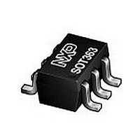
SOT-363
Operating Supply Voltage (max)
3.6V
Operating Supply Voltage (min)
2.3V
Abs. Propagation Delay Time
11.9ns
Mounting
Surface Mount
Pin Count
6
Operating Temperature (min)
-40C
Operating Temperature (max)
125C
Operating Temperature Classification
Automotive
Lead Free Status / RoHS Status
Compliant


NXP Semiconductors
6. Pinning information
Table 3.
7. Functional description
Table 4.
[1]
74AUP1T97
Product data sheet
Symbol
B
GND
A
Y
V
C
Input
C
L
L
L
L
H
H
H
H
Fig 2.
CC
H = HIGH voltage level; L = LOW voltage level.
GND
B
A
Pin configuration SOT363
Pin description
Function table
1
2
3
74AUP1T97
6.1 Pinning
6.2 Pin description
001aag500
Pin
1
2
3
4
5
6
[1]
6
5
4
C
V
Y
B
L
L
H
H
L
L
H
H
CC
Description
data input
ground (0 V)
data input
data output
supply voltage
data input
All information provided in this document is subject to legal disclaimers.
Fig 3.
Rev. 2 — 18 October 2010
GND
Pin configuration SOT886
B
A
Transparent top view
Low-power configurable gate with voltage-level translator
74AUP1T97
1
2
3
A
L
H
L
H
L
H
L
H
001aag501
6
5
4
C
V
Y
CC
Fig 4.
GND
Pin configuration SOT891,
SOT1115 and SOT1202
Output
Y
L
L
H
H
L
H
L
H
B
A
Transparent top view
74AUP1T97
74AUP1T97
1
2
3
© NXP B.V. 2010. All rights reserved.
001aag502
6
5
4
C
V
Y
CC
3 of 20
Related parts for 74AUP1T97GW
Image
Part Number
Description
Manufacturer
Datasheet
Request
R

Part Number:
Description:
NXP Semiconductors designed the LPC2420/2460 microcontroller around a 16-bit/32-bitARM7TDMI-S CPU core with real-time debug interfaces that include both JTAG andembedded trace
Manufacturer:
NXP Semiconductors
Datasheet:

Part Number:
Description:
NXP Semiconductors designed the LPC2458 microcontroller around a 16-bit/32-bitARM7TDMI-S CPU core with real-time debug interfaces that include both JTAG andembedded trace
Manufacturer:
NXP Semiconductors
Datasheet:
Part Number:
Description:
NXP Semiconductors designed the LPC2468 microcontroller around a 16-bit/32-bitARM7TDMI-S CPU core with real-time debug interfaces that include both JTAG andembedded trace
Manufacturer:
NXP Semiconductors
Datasheet:
Part Number:
Description:
NXP Semiconductors designed the LPC2470 microcontroller, powered by theARM7TDMI-S core, to be a highly integrated microcontroller for a wide range ofapplications that require advanced communications and high quality graphic displays
Manufacturer:
NXP Semiconductors
Datasheet:
Part Number:
Description:
NXP Semiconductors designed the LPC2478 microcontroller, powered by theARM7TDMI-S core, to be a highly integrated microcontroller for a wide range ofapplications that require advanced communications and high quality graphic displays
Manufacturer:
NXP Semiconductors
Datasheet:
Part Number:
Description:
The Philips Semiconductors XA (eXtended Architecture) family of 16-bit single-chip microcontrollers is powerful enough to easily handle the requirements of high performance embedded applications, yet inexpensive enough to compete in the market for hi
Manufacturer:
NXP Semiconductors
Datasheet:
Part Number:
Description:
The XA-S3 device is a member of Philips Semiconductors? XA(eXtended Architecture) family of high performance 16-bitsingle-chip microcontrollers
Manufacturer:
NXP Semiconductors
Datasheet:

Part Number:
Description:
The NXP BlueStreak LH75401/LH75411 family consists of two low-cost 16/32-bit System-on-Chip (SoC) devices
Manufacturer:
NXP Semiconductors
Datasheet:
Part Number:
Description:
The NXP LPC3130/3131 combine an 180 MHz ARM926EJ-S CPU core, high-speed USB2
Manufacturer:
NXP Semiconductors
Datasheet:
Part Number:
Description:
The NXP LPC3141 combine a 270 MHz ARM926EJ-S CPU core, High-speed USB 2
Manufacturer:
NXP Semiconductors
Part Number:
Description:
The NXP LPC3143 combine a 270 MHz ARM926EJ-S CPU core, High-speed USB 2
Manufacturer:
NXP Semiconductors

Part Number:
Description:
The NXP LPC3152 combines an 180 MHz ARM926EJ-S CPU core, High-speed USB 2
Manufacturer:
NXP Semiconductors
Part Number:
Description:
The NXP LPC3154 combines an 180 MHz ARM926EJ-S CPU core, High-speed USB 2
Manufacturer:
NXP Semiconductors

Part Number:
Description:
Standard level N-channel enhancement mode Field-Effect Transistor (FET) in a plastic package using NXP High-Performance Automotive (HPA) TrenchMOS technology
Manufacturer:
NXP Semiconductors
Datasheet: