ICS83021AMILF IDT, Integrated Device Technology Inc, ICS83021AMILF Datasheet - Page 3
ICS83021AMILF
Manufacturer Part Number
ICS83021AMILF
Description
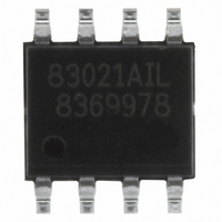
IC FANOUT BUFFER SGL I/O 8-SOIC
Manufacturer
IDT, Integrated Device Technology Inc
Series
HiPerClockS™r
Type
Buffer/Driver, Translatorr
Datasheet
1.ICS83021AMILF.pdf
(12 pages)
Specifications of ICS83021AMILF
Number Of Circuits
1
Ratio - Input:output
1:1
Differential - Input:output
Yes/No
Input
HCSL, LVDS, LVHSTL, LVPECL, SSTL
Output
LVCMOS, LVTTL
Frequency - Max
350MHz
Voltage - Supply
2.375 V ~ 3.6 V
Operating Temperature
-40°C ~ 85°C
Mounting Type
Surface Mount
Package / Case
8-SOIC
Frequency-max
350MHz
Logical Function
Translator
Operating Supply Voltage (typ)
2.5/3.3V
Package Type
SOIC
Operating Supply Voltage (max)
3.6V
Operating Supply Voltage (min)
2.375V
Abs. Propagation Delay Time
2.5ns
Mounting
Surface Mount
Pin Count
8
Operating Temperature (min)
-40C
Operating Temperature (max)
85C
Operating Temperature Classification
Industrial
Lead Free Status / RoHS Status
Lead free / RoHS Compliant
Other names
800-1100
800-1100-5
800-1100
83021AMILF
800-1100-5
800-1100
83021AMILF
Available stocks
Company
Part Number
Manufacturer
Quantity
Price
Company:

Part Number:
ICS83021AMILF
Manufacturer:
ICS
Quantity:
5


Absolute Maximum Ratings
NOTE: Stresses beyond those listed under Absolute Maximum Ratings may cause permanent damage to the device.
These ratings are stress specifications only. Functional operation of product at these conditions or any conditions beyond
those listed in the DC Characteristics or AC Characteristics is not implied. Exposure to absolute maximum rating conditions for
extended periods may affect product reliability.
DC Electrical Characteristics
Table 3A. Power Supply DC Characteristics, V
Table 3B. LVCMOS/LVTTL DC Characteristics, V
NOTE 1: Outputs terminated with 50Ω to V
Table 3C. Differential DC Characteristics, V
NOTE 1: For single ended applications, the maximum input voltage for CLK, nCLK is V
NOTE 2: Common mode voltage is defined as V
IDT™ / ICS™ LVCMOS/LVTTL TRANSLATOR
Item
Supply Voltage, V
Inputs, V
Outputs, V
Package Thermal Impedance, θ
Storage Temperature, T
Symbol
V
I
Symbol
V
V
Symbol
I
I
V
V
DD
IH
IL
ICS83021I
1-TO-1 DIFFERENTIAL-TO-LVCMOS/LVTTL TRANSLATOR
DD
OH
OL
PP
CMR
I
O
Parameter
Output High Voltage; NOTE 1
Output Low Voltage; NOTE 1
Parameter
Input High Current
Input Low Cureent
Peak-to-Peak Input Voltage
Common Mode Input Voltage;
NOTE 1, 2
Parameter
Positive Supply Voltage
Power Supply Current
DD
STG
JA
nCLK
CLK
nCLK
CLK
DD
/2. See Parameter Measurement Information, Output Load Test Circuit Diagrams.
IH
V
V
Test Conditions
.
IN
IN
V
V
DD
IN
IN
= 0V, V
= 0V, V
V
= 3.3V ± 0.3V or 2.5V ± 5%, T
= V
= V
DD
DD
Test Conditions
Test Conditions
DD
V
= 3.6V or 2.625V
DD
DD
= 3.3V ± 0.3V or 2.5V ± 5%, T
V
DD
DD
DD
= 3.3V ± 0.3V or 2.5V ± 5%, T
DD
= 3.6V or 2.625V
= 3.6V or 2.625V
= 2.625V
= 3.6V or 2.625V
= 3.6V or 2.625V
= 3.6V
3
Rating
4.6V
-0.5V to V
-0.5V to V
103°C/W (0 lfpm)
-65°C to 150°C
DD
DD
+ 0.5V
+ 0.5V
Minimum
2.375
Minimum
GND + 0.5
DD
3.0
Minimum
A
1.8
2.6
-150
0.15
= -40°C to 85°C
+ 0.3V.
-5
A
A
= -40°C to 85°C
= -40°C to 85°C
ICS83031AMI REV. C OCTOBER 31, 2008
Typical
Typical
Typical
3.3
2.5
Maximum
Maximum
V
Maximum
DD
2.625
0.5
3.6
150
20
1.3
– 0.85
5
Units
Units
Units
mA
µA
µA
µA
µA
V
V
V
V
V
V
V
Related parts for ICS83021AMILF
Image
Part Number
Description
Manufacturer
Datasheet
Request
R

Part Number:
Description:
TRANSLATION DEVICE DPI 80-PQFP
Manufacturer:
IDT, Integrated Device Technology Inc
Datasheet:
Part Number:
Description:
IDT PART
Manufacturer:
IDT, Integrated Device Technology Inc
Datasheet:
Part Number:
Description:
IC LIU T1/E1/J1 OCTAL 256PBGA
Manufacturer:
IDT, Integrated Device Technology Inc
Datasheet:

Part Number:
Description:
IC FREQ TIMING GENERATOR 28TSSOP
Manufacturer:
IDT, Integrated Device Technology Inc
Datasheet:
Part Number:
Description:
IC CLK DVR PLL 1:10 40VFQFPN
Manufacturer:
IDT, Integrated Device Technology Inc
Datasheet:
Part Number:
Description:
IC CLK FANOUT BUFFER 1:18 32LQFP
Manufacturer:
IDT, Integrated Device Technology Inc
Datasheet:
Part Number:
Description:
IC CLK FANOUT BUFFER 1:18 32LQFP
Manufacturer:
IDT, Integrated Device Technology Inc
Datasheet:
Part Number:
Description:
IC CK505 VREG/RES 56TSSOP
Manufacturer:
IDT, Integrated Device Technology Inc
Datasheet:

Part Number:
Description:
IC SDRAM CLK DVR 1:10 48-TSSOP
Manufacturer:
IDT, Integrated Device Technology Inc
Datasheet:

Part Number:
Description:
IC CLK DVR PLL 1:10 48TSSOP
Manufacturer:
IDT, Integrated Device Technology Inc
Datasheet:
Part Number:
Description:
IC FLEXPC CLK PROGR P4 56-TSSOP
Manufacturer:
IDT, Integrated Device Technology Inc
Datasheet:
Part Number:
Description:
IC FLEXPC CLK PROGR P4 56-TSSOP
Manufacturer:
IDT, Integrated Device Technology Inc
Datasheet:
Part Number:
Description:
IC FLEXPC CLK PROGR P4 56-SSOP
Manufacturer:
IDT, Integrated Device Technology Inc
Datasheet:

Part Number:
Description:
IC PLL CLK DRIVER 2.5V 28-TSSOP
Manufacturer:
IDT, Integrated Device Technology Inc
Datasheet:
Part Number:
Description:
IC CLOCK DRIVER 2.5V 24-TSSOP
Manufacturer:
IDT, Integrated Device Technology Inc
Datasheet: