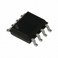
100EL11MX Fairchild Semiconductor, 100EL11MX Datasheet - Page 3

100EL11MX
Manufacturer Part Number
100EL11MX
Description
IC FANOUT BUFFER 5V ECL 8SOIC
Manufacturer
Fairchild Semiconductor
Series
100ELr
Type
Fanout Buffer (Distribution)r
Datasheet
1.100EL11M.pdf
(5 pages)
Specifications of 100EL11MX
Number Of Circuits
1
Ratio - Input:output
1:2
Differential - Input:output
Yes/Yes
Input
ECL
Output
ECL
Voltage - Supply
4.2 V ~ 5.5 V
Operating Temperature
-40°C ~ 85°C
Mounting Type
Surface Mount
Package / Case
8-SOIC (3.9mm Width)
Lead Free Status / RoHS Status
Lead free / RoHS Compliant
Frequency-max
-
Available stocks
Company
Part Number
Manufacturer
Quantity
Price
Company:
Part Number:
100EL11MX
Manufacturer:
LATTICE
Quantity:
20
f
t
t
t
V
t
I
V
V
V
V
V
I
I
MAX
PLH
SKEW
JITTER
r
EE
IH
IL
100EL NECL DC Electrical Characteristics
Note 6: Input and output parameters vary 1 to 1 with V
Note 7: Outputs are terminated through a 50 Resistor to V
Note 8: V
ferential input signal. Normal operation is obtained if the HIGH level falls within the specified range and the peak-to-peak voltage lies between V
1V.
Note 9: Absolute value of the input HIGH and LOW current should not exceed the absolute value of the stated Min or Max specification.
Note: Devices are designed to meet the DC specifications after thermal equilibrium has been established. Circuit is tested with air flow greater than
500LFPM maintained.
AC Electrical Characteristics
Note 10: V
Note 11: Measured using a 750 mV input swing centered at V
with 50
Note 12: Within-device skew defined as identical transitions on similar paths through a device.
Note 13: Duty cycle skew is the difference between a t
Switching Waveforms
Symbol
, t
Symbol
PP
OH
OL
IH
IL
IHCMR
f
, t
PHL
IHCMR
to V
EE
Maximum Toggle Frequency
Propagation Delay to Output
Within Device Skew (Note 12)
Duty Cycle Skew (Note 13)
Cycle-to-Cycle Jitter
Input Swing
Output Rise Times Q
(20% to 80%)
Power Supply Current
Output HIGH Voltage (Note 7)
Output LOW Voltage (Note 7)
Input HIGH Voltage (Single Ended)
Input LOW Voltage (Single Ended)
Input HIGH Voltage Common Mode
Range (Differential) (Note 8)
Input HIGH Current (Note 9)
Input LOW Current (Note 9)
CC
can vary 0.8V / 0.5V.
minimum varies 1 to 1 with V
2.0V.
Parameter
Parameter
FIGURE 1. Differential to Differential Propagation Delay
EE
. V
Min
135
150
100
FIGURE 2. Differential Output Edge Rates
IHCMR
CC
PLH
Min
1085
1830
1165
1810
maximum varies 1 to 1 with V
0.5
. V
2.5
TBD
TBD
and t
40 C
Typ
260
225
EE
CC
5
5
CC
can vary 0.8V/ 0.5V.
V
PHL
- 1.32V; 50% duty cycle clock source; t
CC
2.0V.
40 C
Typ
1005
1695
26
propagation delay through a device under identical conditions.
1000
Max
385
350
5V; V
Max
1555
1475
150
3
31
880
880
EE
0.4
Min
190
150
100
0.0V or V
CC
. The V
Min
1025
1810
1810
1165
0.5
25 C
2.5
TBD
TBD
Typ
265
225
V
5
5
CC
IHCMR
CC
25 C
Typ
1705
0.0V; V
26
955
Max
340
100
350
20
20
range is referenced to the most positive side of the dif-
0.0V; V
r
t
f
EE
Max
1620
1475
150
250 ps (20% - 80%) at f
31
880
880
Min
215
150
100
0.4
EE
5.0V (Note 6)
5V (Note 10)(Note 11)
85 C
Min
1025
1810
1810
TBD
TBD
1165
0.5
Typ
290
225
2.5
5
5
85 C
1000
Max
www.fairchildsemi.com
Typ
1705
365
350
30
955
20
20
IN
1 MHz. All loading
Units
-1475
GHz
Max
1620
mV
150
ps
ps
ps
ps
880
880
36
0.4
PPMIN
Number
Figure 1
Figure 1
Figure 2
Figure
Units
and
mV
mA
mV
mV
mV
V
A
A


