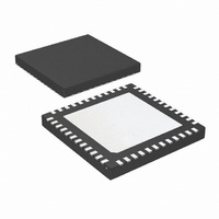
LMK03000CISQ/NOPB National Semiconductor, LMK03000CISQ/NOPB Datasheet - Page 17

LMK03000CISQ/NOPB
Manufacturer Part Number
LMK03000CISQ/NOPB
Description
IC CLOCK CONDITIONER PREC 48-LLP
Manufacturer
National Semiconductor
Type
Clock Conditionerr
Datasheet
1.LMK03000DISQENOPB.pdf
(30 pages)
Specifications of LMK03000CISQ/NOPB
Pll
Yes
Input
Clock
Output
LVDS, LVPECL
Number Of Circuits
1
Ratio - Input:output
1:8
Differential - Input:output
Yes/Yes
Frequency - Max
1.296GHz
Divider/multiplier
Yes/No
Voltage - Supply
3.15 V ~ 3.45 V
Operating Temperature
-40°C ~ 85°C
Mounting Type
Surface Mount
Package / Case
48-LLP
Frequency-max
1.296GHz
For Use With
LMK03000CEVAL - BOARD EVALUATION LMK03000C
Lead Free Status / RoHS Status
Lead free / RoHS Compliant
Other names
LMK03000CISQ
LMK03000CISQTR
LMK03000CISQTR
2.3 REGISTER R0 to R7
Registers R0 through R7 control the eight clock outputs. Reg-
ister R0 controls CLKout0, Register R1 controls CLKout1, and
so on. There is one additional bit in register R0 called RESET.
Default Register Settings after Power on Reset
2.3.1 RESET bit -- R0 only
This bit is only in register R0. The use of this bit is optional
and it should be set to '0' if not used. Setting this bit to a '1'
forces all registers to their power on reset condition and there-
fore automatically clears this bit. If this bit is set, all other R0
bits are ignored and R0 needs to be programmed again if
used with its proper values and RESET = 0.
2.3.2 CLKoutX_MUX[1:0] -- Clock Output Multiplexers
These bits control the Clock Output Multiplexer for each clock
output. Changing between the different modes changes the
blocks in the signal path and therefore incurs a delay relative
to the bypass mode. The different MUX modes and associ-
ated delays are listed below.
RESET
CLKoutX_MUX
CLKoutX_EN
CLKoutX_DIV
CLKoutX_DLY
Vboost
DIV4
OSCin_FREQ
VCO_R4_LF
VCO_R3_LF
VCO_C3_C4_LF
EN_Fout
EN_CLKout_Global
POWERDOWN
PLL_MUX
PLL_R
PLL_CP_GAIN
VCO_DIV
PLL_N
CLKoutX_MUX
[1:0]
Bit Name
0
1
2
3
Divided and
Bypassed
(default)
Delayed
Delayed
Divided
Mode
Bit Value
Default
760
10
10
0
0
0
1
0
0
0
0
0
0
0
1
0
0
0
2
Added Delay Relative
No reset, normal operation
Bypassed
Disabled
Divide by 2
0 ps
Normal Mode
PDF
10 MHz OSCin
Low (~200 Ω)
Low (~600 Ω)
C3 = 0 pF, C4 = 10 pF
Fout disabled
Normal - CLKouts normal
Normal - Device active
Disabled
R divider = 10
100 µA
Divide by 2
N divider = 760
programmed delay)
programmed delay)
to Bypass Mode
(In addition to the
(In addition to the
≤
100 ps
400 ps
500 ps
20 MHz
0 ps
Bit State
17
Aside from this, the functions of these bits are identical. The
X in CLKoutX_MUX, CLKoutX_DIV, CLKoutX_DLY, and
CLKoutX_EN denote the actual clock output which may be
from 0 to 7.
2.3.3 CLKoutX_DIV[7:0] -- Clock Output Dividers
These bits control the clock output divider value. In order for
these dividers to be active, the respective CLKoutX_MUX bit
must be set to either "Divided" or "Divided and Delayed"
mode. After all the dividers are programed, the SYNC* pin
must be used to ensure that all edges of the clock outputs are
aligned. The Clock Output Dividers follow the VCO Divider so
the final clock divide for an output is VCO Divider × Clock
Output Divider. By adding the divider block to the output path
a fixed delay of approximately 100 ps is incurred.
The actual Clock Output Divide value is twice the binary value
programmed as listed in the table below.
Reset to power on defaults
CLKoutX mux mode
CLKoutX enable
CLKoutX clock divide
CLKoutX clock delay
Output Power Control
Phase Detector Frequency
OSCin Frequency in MHz
R4 internal loop filter values
R3 internal loop filter values
C3 and C4 internal loop filter values
Fout enable
Global clock output enable
Device power down
Multiplexer control for LD pin
PLL R divide value
Charge pump current
VCO divide value
PLL N divide value
0
0
0
0
0
0
1
.
0
0
0
0
0
0
1
.
Bit Description
CLKoutX_DIV[7:0]
0
0
0
0
0
0
1
.
0
0
0
0
0
0
1
.
0
0
0
0
0
0
1
.
0
0
0
0
1
1
1
.
0
0
1
1
0
0
1
.
Register
R0 to R7
0
1
0
1
0
1
1
.
R11
R13
R14
R15
R0
R9
Clock Output
Divider value
2 (default)
www.national.com
Invalid
Location
510
10
...
4
6
8
18:17
21:14
13:11
23:20
31:30
29:26
15:8
10:8
19:8
25:8
Bit
7:4
7:4
31
16
16
15
28
27
26


