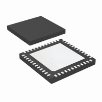
LMK03000CISQ/NOPB National Semiconductor, LMK03000CISQ/NOPB Datasheet - Page 19

LMK03000CISQ/NOPB
Manufacturer Part Number
LMK03000CISQ/NOPB
Description
IC CLOCK CONDITIONER PREC 48-LLP
Manufacturer
National Semiconductor
Type
Clock Conditionerr
Datasheet
1.LMK03000DISQENOPB.pdf
(30 pages)
Specifications of LMK03000CISQ/NOPB
Pll
Yes
Input
Clock
Output
LVDS, LVPECL
Number Of Circuits
1
Ratio - Input:output
1:8
Differential - Input:output
Yes/Yes
Frequency - Max
1.296GHz
Divider/multiplier
Yes/No
Voltage - Supply
3.15 V ~ 3.45 V
Operating Temperature
-40°C ~ 85°C
Mounting Type
Surface Mount
Package / Case
48-LLP
Frequency-max
1.296GHz
For Use With
LMK03000CEVAL - BOARD EVALUATION LMK03000C
Lead Free Status / RoHS Status
Lead free / RoHS Compliant
Other names
LMK03000CISQ
LMK03000CISQTR
LMK03000CISQTR
2.7.3 VCO_R4_LF[2:0] -- Value for Internal Loop Filter
Resistor R4
These bits control the R4 resistor value in the internal loop
filter. The recommended setting for VCO_R4_LF[2:0] = 0 for
optimum phase noise and jitter.
2.7.4 OSCin_FREQ[7:0] -- Oscillator Input Calibration
Adjustment
These bits are to be programmed to the OSCin frequency. If
the OSCin frequency is not an integral multiple of 1 MHz, then
round to the closest value.
2.8 REGISTER R14
2.8.1 PLL_R[11:0] -- R Divider Value
These bits program the PLL R Divider and are programmed
in binary fashion. Any changes to PLL_R require R15 to be
programmed again to active the frequency calibration routine.
0
0
0
0
1
.
.
OSCin_FREQ[7:0]
VCO_R4_LF[2:0]
0
0
0
0
1
.
.
201 to 255
0
0
0
0
1
.
.
5 to 7
200
10
...
...
0
1
2
3
4
1
2
0
0
0
0
1
.
.
PLL_R[11:0]
0
0
0
0
1
.
.
0
0
0
0
1
.
.
0
0
0
0
1
.
.
0
0
0
0
1
.
.
0
0
0
1
1
Low (~200 Ω) (default)
.
.
OSCin Frequency
10 MHz (default)
0
0
0
0
1
.
.
R4 Value (kΩ)
200 MHz
0
0
1
1
1
.
.
Invalid
1 MHz
2 MHz
Invalid
10
20
30
40
...
...
0
1
0
0
1
.
.
PLL R Divide
10 (default)
Invalid
Value
4095
...
...
1
2
19
2.8.2 PLL_MUX[3:0] -- Multiplexer Control for LD Pin
These bits set the output mode of the LD pin. The table below
lists several different modes.
"Logic High" and "Logic Low" allow the PLL_MUX pin to be
used as a general purpose output. These modes are also
useful when debugging to verify programming. The Digital
Lock Detect operation is covered in
TECT.
Analog Lock Detect outputs the state of the charge pump on
the LD pin. While the charge pump is on, the LD pin is low.
While the charge pump is off, the LD pin is high. By using two
resistors, a capacitor, diode, and comparator a lock detect
circuit may be constructed
pump will only turn on momentarily once every period of the
phase detector frequency. "N Divider Output/2" and "R Di-
vider Output/2" output half the frequency of the phase detec-
tor on the LD pin. When the device is locked, these
frequencies should be the same. These options are useful for
debugging.
Note 20: For more information on lock detect circuits, see chapter 32 of PLL
Performance, Simulation and Design Handbook, Fourth Edition by Dean
Banerjee.
PLL_MUX[3:0]
12 to 15
10
11
0
1
2
3
4
5
6
7
8
9
Output Type
Open Drain
Open Drain
Push-Pull
Push-Pull
Push-Pull
Push-Pull
Push-Pull
Push-Pull
Push-Pull
NMOS
PMOS
Hi-Z
(Note
20). When in lock the charge
1.11 DIGITAL LOCK DE-
Invalid
Invalid
Invalid
Analog Lock Detect
Analog Lock Detect
Analog Lock Detect
Digital Lock Detect
Digital Lock Detect
N Divider Output/2
R Divider Output/2
Disabled (default)
(50% Duty Cycle)
(50% Duty Cycle)
LD Pin Function
(Active High)
(Active Low)
Logic High
Logic Low
www.national.com


