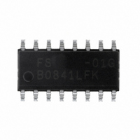
FS6370-01G-XTD ON Semiconductor, FS6370-01G-XTD Datasheet - Page 3

FS6370-01G-XTD
Manufacturer Part Number
FS6370-01G-XTD
Description
IC CLOCK GEN 3-PLL EEPROM 16SOIC
Manufacturer
ON Semiconductor
Type
PLL Clock Generatorr
Datasheet
1.FS6370-01G-XTD.pdf
(28 pages)
Specifications of FS6370-01G-XTD
Pll
Yes
Input
Crystal
Output
CMOS
Number Of Circuits
1
Ratio - Input:output
1:4
Differential - Input:output
No/No
Frequency - Max
230MHz
Divider/multiplier
Yes/No
Voltage - Supply
3 V ~ 5.5 V
Operating Temperature
0°C ~ 70°C
Mounting Type
Surface Mount
Package / Case
16-SOIC (3.9mm Width)
Frequency-max
230MHz
Mounting Style
SMD/SMT
Max Input Freq
230 MHz
Max Output Freq
27 MHz
Number Of Outputs
1
Operating Supply Voltage
5 V to 3.3 V
Operating Temperature Range
0 C to + 70 C
Supply Current
43 mA
Lead Free Status / RoHS Status
Lead free / RoHS Compliant
Other names
766-1025
Available stocks
Company
Part Number
Manufacturer
Quantity
Price
Company:
Part Number:
FS6370-01G-XTD
Manufacturer:
ON Semiconductor
Quantity:
38
FS6370
3.0 Functional Block Description
3.1 Phase Locked Loops (PLLs)
Each of the three on-chip PLLs is a standard phase- and frequency-locked loop architecture that multiplies a reference frequency to a
desired frequency by a ratio of integers. This frequency multiplication is exact.
As shown in Figure 3, each PLL consists of a reference divider, a phase-frequency detector (PFD), a charge pump, an internal loop
filter, a voltage-controlled oscillator (VCO), and a feedback divider.
During operation, the reference frequency (f
), generated by the on-board crystal oscillator, is first reduced by the reference divider.
REF
The divider value is often referred to as the modulus, and is denoted as N
for the reference divider. The divided reference is fed into
R
the PFD.
The PFD controls the frequency of the VCO (f
) through the charge pump and loop filter. The VCO provides a high-speed, low noise,
VCO
continuously variable frequency clock source for the PLL. The output of the VCO is fed back to the PFD through the feedback divider
(the modulus is denoted by N
) to close the loop.
F
Figure 3: PLL Block Diagram
The PFD will drive the VCO up or down in frequency until the divided reference frequency and the divided VCO frequency appearing at
the inputs of the PFD are equal. The input/output relationship between the reference frequency and the VCO frequency is:
3.1.1. Reference Divider
The reference divider is designed for low phase jitter. The divider accepts the output of the reference oscillator and provides a divided-
down frequency to the PFD. The reference divider is an 8-bit divider, and can be programmed for any modulus from 1 to 255 by
programming the equivalent binary value. A divide-by-256 can also be achieved by programming the eight bits to 00h.
3.1.2. Feedback Divider
The feedback divider is based on a dual-modulus pre-scaler technique. The technique allows the same granularity as a fully
programmable feedback divider, while still allowing the programmable portion to operate at low speed. A high-speed pre-divider (also
called a pre-scaler) is placed between the VCO and the programmable feedback divider because of the high speeds at which the VCO
can operate. The dual-modulus technique insures reliable operation at any speed that the VCO can achieve and reduces the overall
power consumption of the divider.
For example, a fixed divide-by-eight pre-scaler could have been used in the feedback divider. Unfortunately, a divide-by-eight would
limit the effective modulus of the entire feedback divider to multiples of eight. This limitation would restrict the ability of the PLL to
Rev. 3 | Page 3 of 28 | www.onsemi.com


