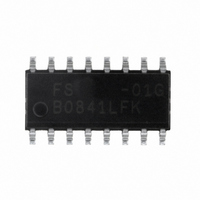
FS6370-01G-XTD ON Semiconductor, FS6370-01G-XTD Datasheet - Page 8

FS6370-01G-XTD
Manufacturer Part Number
FS6370-01G-XTD
Description
IC CLOCK GEN 3-PLL EEPROM 16SOIC
Manufacturer
ON Semiconductor
Type
PLL Clock Generatorr
Datasheet
1.FS6370-01G-XTD.pdf
(28 pages)
Specifications of FS6370-01G-XTD
Pll
Yes
Input
Crystal
Output
CMOS
Number Of Circuits
1
Ratio - Input:output
1:4
Differential - Input:output
No/No
Frequency - Max
230MHz
Divider/multiplier
Yes/No
Voltage - Supply
3 V ~ 5.5 V
Operating Temperature
0°C ~ 70°C
Mounting Type
Surface Mount
Package / Case
16-SOIC (3.9mm Width)
Frequency-max
230MHz
Mounting Style
SMD/SMT
Max Input Freq
230 MHz
Max Output Freq
27 MHz
Number Of Outputs
1
Operating Supply Voltage
5 V to 3.3 V
Operating Temperature Range
0 C to + 70 C
Supply Current
43 mA
Lead Free Status / RoHS Status
Lead free / RoHS Compliant
Other names
766-1025
Available stocks
Company
Part Number
Manufacturer
Quantity
Price
Company:
Part Number:
FS6370-01G-XTD
Manufacturer:
ON Semiconductor
Quantity:
38
FS6370
7.2 Non-Programming Migration Path
If the design has solidified on a particular EEPROM programming pattern, the EEPROM pattern can be hard-coded into a ROM-based
device. For high-volume requirements, a ROM-based device offers significant cost savings over the FS6370. Contact an ON
Semiconductor sales representative for more detail.
8.0 I
I
V
8.1 Bus Conditions
Data transfer on the bus can only be initiated when the bus is not busy. During the data transfer, the data line (SDA) must remain stable
whenever the clock line (SCL) is high. Changes in the data line while the clock line is high will be interpreted by the device as a START
or STOP condition. The following bus conditions are defined by the I
8.1.1. Not Busy
Both the data (SDA) and clock (SCL) lines remain high to indicate the bus is not busy.
8.1.2. START Data Transfer
A high to low transition of the SDA line while the SCL input is high indicates a START condition. All commands to the device must be
preceded by a START condition.
2
C-bus logic levels noted herein are based on a percentage of the power supply (V
DD
, while a logic-low corresponds to ground (V
2
C-bus Control Interface
This device is a read/write slave device meeting all Philips I
be controlled by a master device that generates the serial clock SCL, controls bus access and generates the START and
STOP conditions while the device works as a slave. Both master and slave can operate as a transmitter or receiver, but
the master device determines which mode is activated. A device that sends data onto the bus is defined as the
transmitter, and a device receiving data as the receiver.
SS
).
Rev. 3 | Page 8 of 28 | www.onsemi.com
Figure 5: FS6370 to FS6377
2
C-bus protocol.
2
C-bus specifications except a "general call." The bus has to
DD
). A logic-one corresponds to a nominal voltage of


