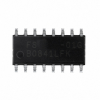
FS6370-01G-XTD ON Semiconductor, FS6370-01G-XTD Datasheet - Page 7

FS6370-01G-XTD
Manufacturer Part Number
FS6370-01G-XTD
Description
IC CLOCK GEN 3-PLL EEPROM 16SOIC
Manufacturer
ON Semiconductor
Type
PLL Clock Generatorr
Datasheet
1.FS6370-01G-XTD.pdf
(28 pages)
Specifications of FS6370-01G-XTD
Pll
Yes
Input
Crystal
Output
CMOS
Number Of Circuits
1
Ratio - Input:output
1:4
Differential - Input:output
No/No
Frequency - Max
230MHz
Divider/multiplier
Yes/No
Voltage - Supply
3 V ~ 5.5 V
Operating Temperature
0°C ~ 70°C
Mounting Type
Surface Mount
Package / Case
16-SOIC (3.9mm Width)
Frequency-max
230MHz
Mounting Style
SMD/SMT
Max Input Freq
230 MHz
Max Output Freq
27 MHz
Number Of Outputs
1
Operating Supply Voltage
5 V to 3.3 V
Operating Temperature Range
0 C to + 70 C
Supply Current
43 mA
Lead Free Status / RoHS Status
Lead free / RoHS Compliant
Other names
766-1025
Available stocks
Company
Part Number
Manufacturer
Quantity
Price
Company:
Part Number:
FS6370-01G-XTD
Manufacturer:
ON Semiconductor
Quantity:
38
FS6370
If a stop bit is transmitted before the entire write command sequence is complete, then the command is aborted and no data is written
to memory. If more than eight bits are transmitted before the stop bit is sent, then the EEPROM will clear the previously loaded data
byte and will begin loading the data buffer again.
6.1.2. Acknowledge Polling
The EEPROM does not acknowledge while it internally commits data to memory. This feature can be used to increase data throughput
by determining when the internal write cycle is complete.
The process is to initiate the random register write procedure with a START condition, the EEPROM device address, and the write
command bit (R/W=0).
If the EEPROM has completed its internal 4 ms write cycle, the EEPROM will acknowledge on the next clock, and the write command
can continue.
If the EEPROM has not completed the internal 4 ms write cycle, the random register write procedure must be restarted by sending the
START condition, device address and R/W bit. This sequence must be repeated until the EEPROM acknowledges.
6.1.3. Read Operation
The EEPROM supports both the random register read procedure and the sequential register read procedure (both are outlined in
Section 6).
For sequential read operations, the EEPROM has an internal address pointer that increments by one at the end of each read operation.
The pointer directs the EEPROM to transmit the next sequentially addressed data byte, allowing the entire memory contents to be read
in one operation.
6.2 Direct Register Programming
The FS6370 control registers may be directly accessed by simply using the FS6370 device address in the read or write operations. The
operation of the device will follow the register values. The register map of the FS6370 is identical to that of the EEPROM shown in
Table 3.
The FS6370 supports the random read and write procedures, as well as the sequential read and write procedures described in Section
8.
The device address for the FS6370 is:
7.0 Cost Reduction Migration Path
The FS6370 is compatible with the programmable register-based FS6377 or a fixed-frequency ROM-based clock generator. Attention
should be paid to the board layout if a migration path to either of these devices is desired.
7.1 Programming Migration Path
If the design can support I
is possible.
Figure 5 shows the five pins that may not be compatible between the various devices if programming of the FS6370 or the FS6377 is
desired.
A6
1
A5
0
2
C programming overhead, a cost reduction from the EEPROM-based FS6370 to the register-based FS6377
A4
1
Rev. 3 | Page 7 of 28 | www.onsemi.com
A3
1
A2
1
A1
0
A0
0


