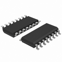
74HCT9046AD,118 NXP Semiconductors, 74HCT9046AD,118 Datasheet - Page 34

74HCT9046AD,118
Manufacturer Part Number
74HCT9046AD,118
Description
IC PLL BAND GAP CNTRL VCO 16SOIC
Manufacturer
NXP Semiconductors
Type
Phase Lock Loop (PLL)r
Series
74HCTr
Datasheet
1.74HCT9046AD118.pdf
(43 pages)
Specifications of 74HCT9046AD,118
Number Of Circuits
1
Package / Case
16-SOIC (3.9mm Width)
Pll
Yes
Input
Clock
Output
Clock
Ratio - Input:output
2:2
Differential - Input:output
No/No
Frequency - Max
16MHz
Divider/multiplier
No/No
Voltage - Supply
4.5 V ~ 5.5 V
Operating Temperature
-40°C ~ 125°C
Mounting Type
Surface Mount
Frequency-max
16MHz
Supply Voltage (max)
5.5 V
Supply Voltage (min)
4.5 V
Maximum Operating Temperature
+ 125 C
Minimum Operating Temperature
- 40 C
Mounting Style
SMD/SMT
Operating Supply Voltage
4.5 V to 5.5 V
Lead Free Status / RoHS Status
Lead free / RoHS Compliant
Lead Free Status / RoHS Status
Lead free / RoHS Compliant, Lead free / RoHS Compliant
Other names
568-1570-2
74HCT9046AD-T
935044180118
74HCT9046AD-T
935044180118
NXP Semiconductors
74HCT9046A_6
Product data sheet
Using PC2 with the passive filter as shown in
same performance as a loop with an active filter. Hence loop filter equations as for a high
gain loop should be used. The current source output of PC2 can be simulated then with a
fictive filter resistance:
The transfer functions of the filter is given by:
Where:
The characteristic equation is:
This results in:
or:
This can be written as:
with the natural frequency
and the damping value given as:
In
The overshoot and settling time percentages are now used to determine
From
of less than 20 % and settle to within 5 % at
This results in:
K
R3‘
K
1
s
s
2
2
1
2
+
n
p
f
Figure 35
+
+
=
=
K
=
=
=
sK
2
=
p
R3‘ C2
R4 C2
Figure 35
1
---------------- -
----------- -
4
p
R
----------- -
1
---------------- -
K
-------------------------------- -
+
s
5
K
17
n
bias
+
s
s
p
s
v
2
K
+
s
1
2
=
n
the output frequency response to a step of input frequency is shown.
K
2
---- -
1
v
0.4 V r
2
1
K
----- - K
n
it can be seen that the damping ratio = 0.707 will produce an overshoot
s
+
v
2
K
K
=
n
n
p
Rev. 06 — 15 September 2009
K
0
=
v
0
K
n
n
1
defined as:
=
1
0
+
K
=
p
0.5
K
f
2
K
Figure 34
n
o
t = 5. The required settling time is 1 ms.
n
K
n
PLL with band gap controlled VCO
results in a high gain loop with the
74HCT9046A
© NXP B.V. 2009. All rights reserved.
n
.
34 of 43


