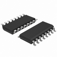
74HCT9046AD,118 NXP Semiconductors, 74HCT9046AD,118 Datasheet - Page 6

74HCT9046AD,118
Manufacturer Part Number
74HCT9046AD,118
Description
IC PLL BAND GAP CNTRL VCO 16SOIC
Manufacturer
NXP Semiconductors
Type
Phase Lock Loop (PLL)r
Series
74HCTr
Datasheet
1.74HCT9046AD118.pdf
(43 pages)
Specifications of 74HCT9046AD,118
Number Of Circuits
1
Package / Case
16-SOIC (3.9mm Width)
Pll
Yes
Input
Clock
Output
Clock
Ratio - Input:output
2:2
Differential - Input:output
No/No
Frequency - Max
16MHz
Divider/multiplier
No/No
Voltage - Supply
4.5 V ~ 5.5 V
Operating Temperature
-40°C ~ 125°C
Mounting Type
Surface Mount
Frequency-max
16MHz
Supply Voltage (max)
5.5 V
Supply Voltage (min)
4.5 V
Maximum Operating Temperature
+ 125 C
Minimum Operating Temperature
- 40 C
Mounting Style
SMD/SMT
Operating Supply Voltage
4.5 V to 5.5 V
Lead Free Status / RoHS Status
Lead free / RoHS Compliant
Lead Free Status / RoHS Status
Lead free / RoHS Compliant, Lead free / RoHS Compliant
Other names
568-1570-2
74HCT9046AD-T
935044180118
74HCT9046AD-T
935044180118
NXP Semiconductors
8. Functional description
74HCT9046A_6
Product data sheet
8.1 Differences with respect to the familiar 74HCT4046A
The 74HCT9046A is a phase-locked-loop circuit that comprises a linear VCO and two
different phase comparators (PC1 and PC2) with a common signal input amplifier and a
common comparator input, see
voltage signals (CMOS level), or indirectly coupled (with a series capacitor) to small
voltage signals. A self-bias input circuit keeps small voltage signals within the linear region
of the input amplifiers. With a passive low-pass filter, the 74HCT9046A forms a
second-order loop PLL.
The principle of this phase-locked-loop is based on the familiar 74HCT4046A. However
extra features are built-in, allowing very high-performance phase-locked-loop applications.
This is done, at the expense of PC3, which is skipped in this 74HCT9046A. The PC2 is
equipped with a current source output stage here. Further a band gap is applied for all
internal references, allowing a small center frequency tolerance. The details are summed
up in
section only.
•
•
•
•
•
•
•
•
A center frequency tolerance of maximum 10 %.
The on board band gap sets the internal references resulting in a minimal frequency
shift at supply voltage variations and temperature variations.
The value of the frequency offset is determined by an internal reference voltage of
2.5 V instead of V
supply voltage range.
A current switch charge pump output on pin PC2_OUT allows a virtually ideal
performance of PC2; The gain of PC2 is independent of the voltage across the
low-pass filter; Further a passive low-pass filter in the loop achieves an active
performance. The influence of the parasitic capacitance of the PC2 output plays no
role here, resulting in a true correspondence of the output correction pulse and the
phase difference even up to phase differences as small as a few nanoseconds.
Because of its linear performance without dead zone, higher impedance values for the
filter, hence lower C-values, can be chosen; correct operation will not be influenced by
parasitic capacitances as in case of the voltage source output using the
74HCT4046A.
No PC3 on pin RB but instead a resistor connected to GND, which sets the
load/unload currents of the charge pump (PC2).
Extra GND pin 1 to allow an excellent FM demodulator performance even at 10 MHz
and higher.
Combined function of pin PC1_OUT/PCP_OUT. If pin RB is connected to V
bias resistor R
PC1. If at pin RB a resistor (R
been chosen as phase comparator. Connection of R
and this changes the function of pin PC1_OUT/PCP_OUT into a lock detect output
(PCP_OUT) with the same characteristics as PCP_OUT of pin 1 of the 74HCT4046A.
Section
8.1. If one is familiar with the 74HCT4046A already, it will do to read this
bias
Rev. 06 — 15 September 2009
) pin PC1_OUT/PCP_OUT has its familiar function viz. output of
CC
0.7 V; In this way the offset frequency will not shift over the
Figure
bias
) is connected to GND it is assumed that PC2 has
1. The signal input can be directly coupled to large
PLL with band gap controlled VCO
bias
is sensed by internal circuitry
74HCT9046A
© NXP B.V. 2009. All rights reserved.
CC
(no
6 of 43


