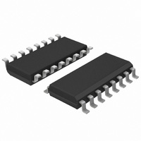
74HCT9046AD,112 NXP Semiconductors, 74HCT9046AD,112 Datasheet - Page 20

74HCT9046AD,112
Manufacturer Part Number
74HCT9046AD,112
Description
IC PLL BAND GAP CNTRL VCO 16SOIC
Manufacturer
NXP Semiconductors
Type
Phase Lock Loop (PLL)r
Series
74HCTr
Datasheet
1.74HCT9046AD118.pdf
(43 pages)
Specifications of 74HCT9046AD,112
Number Of Circuits
1
Package / Case
16-SOIC (3.9mm Width)
Pll
Yes
Input
Clock
Output
Clock
Ratio - Input:output
2:2
Differential - Input:output
No/No
Frequency - Max
16MHz
Divider/multiplier
No/No
Voltage - Supply
4.5 V ~ 5.5 V
Operating Temperature
-40°C ~ 125°C
Mounting Type
Surface Mount
Frequency-max
16MHz
Maximum Input Frequency
16 MHz
Minimum Input Frequency
11 MHz
Output Frequency Range
2 MHz to 3 MHz
Supply Voltage (max)
5.5 V
Supply Voltage (min)
4.5 V
Maximum Operating Temperature
+ 125 C
Minimum Operating Temperature
- 40 C
Mounting Style
SMD/SMT
Operating Supply Voltage
5 V
Lead Free Status / RoHS Status
Lead free / RoHS Compliant
Lead Free Status / RoHS Status
Lead free / RoHS Compliant, Lead free / RoHS Compliant
Other names
568-3978-5
74HCT9046AD
74HCT9046AD
935044180112
74HCT9046AD
74HCT9046AD
935044180112
NXP Semiconductors
12. Dynamic characteristics
Table 6.
GND = 0 V; t
74HCT9046A_6
Product data sheet
Symbol
T
Phase comparator section
t
t
t
t
V
VCO section
f
General
C
T
Phase comparator section
t
t
t
t
VCO section
pd
en
dis
t
0
pd
en
dis
t
amb
f
f/f
amb
i(p-p)
PD
= 25 C
= 40 C to +85 C
Dynamic characteristics
r
= t
Parameter
propagation delay
enable time
disable time
transition time
peak-to-peak input voltage
frequency deviation
center frequency
relative frequency variation
duty cycle
power dissipation capacitance
propagation delay
enable time
disable time
transition time
f
= 6 ns; C
L
= 50 pF.
[1]
Rev. 06 — 15 September 2009
Conditions
SIG_IN, COMP_IN to PC1_OUT;
V
SIG_IN, COMP_IN to PCP_OUT;
V
SIG_IN, COMP_IN to PC2_OUT;
V
SIG_IN, COMP_IN to PC2_OUT;
V
V
pin SIGN_IN or COMP_IN;
V
V
R1 = 10 k ; R2 = 10 k ; C1 = 1 nF
V
V
R2 =
and
V
V
R2 =
and
V
C1 = 100 pF; see
VCO_OUT; V
SIG_IN, COMP_IN to PC1_OUT;
V
SIG_IN, COMP_IN to PCP_OUT;
V
SIG_IN, COMP_IN to PC2_OUT;
V
SIG_IN, COMP_IN to PC2_OUT;
V
V
CC
CC
CC
CC
CC
CC
CC
CC
VCO_IN
CC
VCO_IN
CC
CC
CC
CC
CC
CC
= 4.5 V; see
= 4.5 V; see
31
31
= 4.5 V; see
= 4.5 V; see
= 4.5 V; see
= 4.5 V; AC coupled; f
= 5.0 V; V
= 4.5 V; duty cycle = 50 %;
= 5 V; duty cycle = 50 %;
= 4.5 V; R1 = 100 k ; R2 =
= 4.5 V; see
= 4.5 V; see
= 4.5 V; see
= 4.5 V; see
= 4.5 V; see
= 0.5V
= 0.5V
; C1 = 40 pF; see
; C1 = 40 pF; see
CC
VCO_IN
CC
CC
= 4.5 V
Figure 19
Figure 19
Figure 18
Figure 18
Figure 18
Figure 18
Figure 18
Figure 19
Figure 19
Figure 18
; R1 = 4.3 k ;
; R1 = 3 k ;
Figure 24
= 3.9 V;
i
= 1 MHz
Figure 23
Figure 23
and
25
PLL with band gap controlled VCO
;
[2][3]
[4]
[5]
[6]
74HCT9046A
Min
-
-
-
-
-
-
11.0
-
-
-
-
-
-
-
-
-
10
Typ
23
35
30
36
7
50
-
15.0
16.0
0.4
50
20
-
-
-
-
-
© NXP B.V. 2009. All rights reserved.
Max
40
68
56
65
15
-
+10
-
-
-
-
-
50
85
70
81
19
20 of 43
Unit
ns
ns
ns
ns
ns
mV
%
MHz
MHz
%
%
pF
ns
ns
ns
ns
ns


