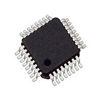
IDT5V9885PFGI IDT, Integrated Device Technology Inc, IDT5V9885PFGI Datasheet - Page 29

IDT5V9885PFGI
Manufacturer Part Number
IDT5V9885PFGI
Description
IC CLK GEN 3.3V EEPROM 32-TQFP
Manufacturer
IDT, Integrated Device Technology Inc
Type
Clock Generatorr
Datasheet
1.IDT5V9885NLGI.pdf
(37 pages)
Specifications of IDT5V9885PFGI
Pll
Yes with Bypass
Input
LVCMOS, LVTTL, Crystal
Output
LVCMOS, LVDS, LVPECL, LVTTL
Number Of Circuits
1
Ratio - Input:output
2:8
Differential - Input:output
No/Yes
Frequency - Max
500MHz
Divider/multiplier
Yes/Yes
Voltage - Supply
3.135 V ~ 3.6 V
Operating Temperature
-40°C ~ 85°C
Mounting Type
Surface Mount
Package / Case
32-TQFP, 32-VQFP
Frequency-max
500MHz
Number Of Elements
3
Supply Current
120mA
Pll Input Freq (min)
1MHz
Pll Input Freq (max)
400MHz
Operating Supply Voltage (typ)
3.3V
Operating Temp Range
-40C to 85C
Package Type
TQFP
Output Frequency Range
0.0049 to 500MHz
Operating Supply Voltage (min)
3V
Operating Supply Voltage (max)
3.6V
Operating Temperature Classification
Industrial
Pin Count
32
Lead Free Status / RoHS Status
Lead free / RoHS Compliant
Other names
5V9885PFGI
800-1992
IDT5V9885PFGI
800-1992
IDT5V9885PFGI
Available stocks
Company
Part Number
Manufacturer
Quantity
Price
Company:
Part Number:
IDT5V9885PFGI
Manufacturer:
IDT
Quantity:
513
Company:
Part Number:
IDT5V9885PFGI
Manufacturer:
IDT, Integrated Device Technology Inc
Quantity:
10 000
Part Number:
IDT5V9885PFGI
Manufacturer:
IDT
Quantity:
20 000
Company:
Part Number:
IDT5V9885PFGI8
Manufacturer:
IDT, Integrated Device Technology Inc
Quantity:
10 000
DC ELECTRICAL CHARACTERISTICS FOR LVDS
NOTES:
1. Output banks 4 and 5 are toggling. Other output banks are powered down.
2. The termination resistors are excluded from these measurements.
NOTES:
1. Output banks 4 and 5 are toggling. Other output banks are powered down.
2. The termination resistors are excluded from these measurements.
POWER SUPPLY CHARACTERISTICS FOR LVDS OUTPUTS
DC ELECTRICAL CHARACTERISTICS FOR LVPECL
POWER SUPPLY CHARACTERISTICS FOR LVPECL OUTPUTS
IDT5V9885
3.3V EEPROM PROGRAMMABLE CLOCK GENERATOR
Symbol
Symbol
Symbol
Symbol
V
V
V
Δ V
Δ V
OT
V
I
I
I
V
I
I
OT
I
V
SWING
I
I
OSD
DDQ
DDD
DDQ
DDD
TOT
TOT
OS
OS
OH
OL
(+)
OS
OT
(-)
Quiescent V
Dynamic V
Current per Output
Total Power V
Quiescent V
Dynamic V
Current per Output
Total Power V
Parameter
Differential Output Voltage for the TRUE binary state
Differential Output Voltage for the FALSE binary state
Change in V
Output Common Mode Voltage (Offset Voltage)
Change in V
Outputs Short Circuit Current, V
Differential Outputs Short Circuit Current, V
Output Voltage HIGH, terminated through 50Ω tied to V
Output Voltage LOW, terminated through 50Ω tied to V
Peak to Peak Output Voltage Swing
Parameter
DD
Parameter
DD
Parameter
DD
DD
OT
OS
DD
DD
Power Supply
Power Supply
Power Supply Current
Power Supply Current
between Complimentary Output States
between Complimentary Output States
Supply Current
Supply Current
OUT
+ or V
OUT
OUT
REF = LOW
Outputs enabled, All outputs unloaded
V
F
F
F
REF = LOW
Outputs enabled, All outputs unloaded
V
F
F
F
- = 0V or V
DD
REFERENCE CLOCK
REFERENCE CLOCK
REFERENCE CLOCK
DD
REFERENCE CLOCK
REFERENCE CLOCK
REFERENCE CLOCK
+ = V
= Max., C
= Max., C
OUT
Test Conditions
Test Conditions
DD
-
DD
DD
- 2V
- 2V
L
L
= 0pF
= 0pF
= 100MHz, C
= 200MHz, C
= 400MHz, C
= 100MHz, C
= 200MHz, C
= 400MHz, C
29
(2)
(2)
L
L
L
L
L
L
= 5pf
= 5pf
= 5pf
= 5pf
= 5pf
= 5pf
V
V
DD
DD
1.125
Min.
-247
Min.
0.55
247
—
—
—
—
- 1.95
- 1.2
INDUSTRIAL TEMPERATURE RANGE
(1)
(1)
Typ.
Typ.
Typ.
Typ.
100
122
120
130
140
1.2
—
—
—
—
68
30
86
—
—
—
86
35
9
6
V
V
DD
DD
1.375
Max
-454
Max
Max
0.93
Max
454
130
150
190
110
180
190
210
50
50
24
12
90
45
50
- 1.61
- 0.9
μA/MHz
μA/MHz
Unit
Unit
Unit
Unit
mV
mV
mV
mV
mA
mA
mA
mA
mA
mA
V
V
V
V


