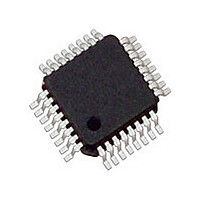
IDT5V9885PFGI IDT, Integrated Device Technology Inc, IDT5V9885PFGI Datasheet - Page 30

IDT5V9885PFGI
Manufacturer Part Number
IDT5V9885PFGI
Description
IC CLK GEN 3.3V EEPROM 32-TQFP
Manufacturer
IDT, Integrated Device Technology Inc
Type
Clock Generatorr
Datasheet
1.IDT5V9885NLGI.pdf
(37 pages)
Specifications of IDT5V9885PFGI
Pll
Yes with Bypass
Input
LVCMOS, LVTTL, Crystal
Output
LVCMOS, LVDS, LVPECL, LVTTL
Number Of Circuits
1
Ratio - Input:output
2:8
Differential - Input:output
No/Yes
Frequency - Max
500MHz
Divider/multiplier
Yes/Yes
Voltage - Supply
3.135 V ~ 3.6 V
Operating Temperature
-40°C ~ 85°C
Mounting Type
Surface Mount
Package / Case
32-TQFP, 32-VQFP
Frequency-max
500MHz
Number Of Elements
3
Supply Current
120mA
Pll Input Freq (min)
1MHz
Pll Input Freq (max)
400MHz
Operating Supply Voltage (typ)
3.3V
Operating Temp Range
-40C to 85C
Package Type
TQFP
Output Frequency Range
0.0049 to 500MHz
Operating Supply Voltage (min)
3V
Operating Supply Voltage (max)
3.6V
Operating Temperature Classification
Industrial
Pin Count
32
Lead Free Status / RoHS Status
Lead free / RoHS Compliant
Other names
5V9885PFGI
800-1992
IDT5V9885PFGI
800-1992
IDT5V9885PFGI
Available stocks
Company
Part Number
Manufacturer
Quantity
Price
Company:
Part Number:
IDT5V9885PFGI
Manufacturer:
IDT
Quantity:
513
Company:
Part Number:
IDT5V9885PFGI
Manufacturer:
IDT, Integrated Device Technology Inc
Quantity:
10 000
Part Number:
IDT5V9885PFGI
Manufacturer:
IDT
Quantity:
20 000
Company:
Part Number:
IDT5V9885PFGI8
Manufacturer:
IDT, Integrated Device Technology Inc
Quantity:
10 000
AC TIMING ELECTRICAL CHARACTERISTICS
(SPREAD SPECTRUM GENERATION = OFF)
NOTES:
1. Practical lower input frequency is determined by loop filter settings.
2. A slew rate of 2V/ns or greater should be selected for output frequencies of 100MHz and higher.
3. Input frequency is the same as the output with all output banks running at the same frequency.
4. Skew measured between all in-phase outputs in the same bank.
5. Skew measured between the cross points of all differential output pairs under identical input and output interfaces, transitions and load conditions on any one device.
6. Includes loading the configuration bits from EEPROM to PLL registers. It does not include EEPROM programming/write time.
7. Guaranteed by design but not production tested.
8. Actual PLL lock time depends on the loop configuration.
NOTE:
1. Practical lower input frequency is determined by loop filter settings.
SPREAD SPECTRUM GENERATION SPECIFICATIONS
IDT5V9885
3.3V EEPROM PROGRAMMABLE CLOCK GENERATOR
Symbol
Symbol
f
SPREAD
1/t1
f
f
f
t4
f
t10
VCO
PFD
MOD
f
BW
t2
t3
t5
t6
t7
t8
t9
f
IN
IN
(2)
Parameter
Input Frequency
Output Frequency
VCO Frequency
PFD Frequency
Loop Bandwidth
Input Duty Cycle
Output Duty Cycle
Slew Rate
SLEWx(bits) = 00
Slew Rate
SLEWx(bits) = 01
Slew Rate
SLEWx(bits) = 10
Slew Rate
SLEWx(bits) = 11
Rise Times
Fall Times
Rise Times
Fall Times
Output three-state Timing
Clock Jitter
Output Skew
Lock Time
Lock time
Parameter
Input Frequency
Mod Freq
Spread Value
(8)
(3,7)
Amount of Spread Value (Programmable) - Center Spread
Amount of Spread Value (Programmable) - Down Spread
VCO operating Frequency Range
Single-Ended Output clock rise and fall time,
Single-Ended Output clock rise and fall time,
Single-Ended Output clock rise and fall time,
Single-Ended Output clock rise and fall time,
Input Frequency Limit
Single Ended Clock output limit (LVTTL)
Differential Clock output limit (LVPECL/ LVDS)
PFD operating Frequency Range
Based on loop filter resistor and capacitor values
Duty Cycle for Input
Measured at V
Measured at V
20% to 80% of V
20% to 80% of V
20% to 80% of V
20% to 80% of V
LVDS, 20% to 80%
LVPECL, 20% to 80%
Time for output to enter or leave three-state mode
after SHUTDOWN/OE switches
Peak-to-peak period jitter,
CLK outputs measured at V
Skew between output to output on the same bank
(bank 4 and bank 5 only)
PLL Lock Time from Power-up
PLL Lock time from shutdown mode
Modulation Frequency
Input Frequency Limit
DD
DD
DD
DD
DD
DD
/2, F
/2, F
Description
(Output Load = 15pf)
(Output Load = 15pf)
(Output Load = 15pf)
(Output Load = 15pf)
OUT
OUT
Test Conditions
(4, 5)
≤ 200MHz
> 200MHz
DD
/2
(6)
30
f
f
PFD
PFD
> 20MHz
< 20MHz
Min.
1
—
(1)
0.0049
0.0049
Min.
0.4
0.03
INDUSTRIAL TEMPERATURE RANGE
-0.5, -1, -2.5, -3.5, -4
1
10
40
45
40
—
—
—
—
—
—
—
—
—
—
—
—
—
—
(1)
(1)
-0.5 to +0.5
Typ.
—
33
Typ.
2.75
1.25
0.75
850
850
500
500
200
—
—
—
—
—
—
—
10
20
—
—
—
—
—
2
Max
1/F
400
—
150 +
1200
Max
400
200
500
400
150
150
100
40
60
55
60
—
—
—
—
—
—
—
20
—
—
OUTX
%f
MHz
MHz
MHz
MHz
MHz
Unit
V/ns
MHz
Unit
kHz
ms
%
%
μs
ps
ns
ps
ps
OUT


