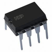
PCF8583P/F5,112 NXP Semiconductors, PCF8583P/F5,112 Datasheet - Page 20

PCF8583P/F5,112
Manufacturer Part Number
PCF8583P/F5,112
Description
IC CLK/CALENDAR 240X8 RAM 8-DIP
Manufacturer
NXP Semiconductors
Type
Clock/Calendar/NVSRAMr
Datasheet
1.PCF8583T5518.pdf
(37 pages)
Specifications of PCF8583P/F5,112
Package / Case
8-DIP (0.300", 7.62mm)
Memory Size
240B
Time Format
HH:MM:SS (12/24 hr)
Date Format
YY-MM-DD
Interface
I²C, 2-Wire Serial
Voltage - Supply
1 V ~ 6 V
Operating Temperature
-40°C ~ 85°C
Mounting Type
Through Hole
Mounting Style
Through Hole
Lead Free Status / RoHS Status
Lead free / RoHS Compliant
Lead Free Status / RoHS Status
Lead free / RoHS Compliant, Lead free / RoHS Compliant
Other names
568-1084-5
935261345112
PCF8583PN
935261345112
PCF8583PN
Available stocks
Company
Part Number
Manufacturer
Quantity
Price
Company:
Part Number:
PCF8583P/F5,112
Manufacturer:
LTC
Quantity:
147
NXP Semiconductors
10. Characteristics
Table 7.
V
[1]
[2]
[3]
[4]
[5]
[6]
[7]
PCF8583
Product data sheet
Symbol
V
I
V
Pin SDA
V
V
I
I
C
Pins A0 and OSCI
I
Pin INT
I
I
Pin SCL
I
C
DD
OL
LI
LI
OL
LI
LI
DD
DD
en
IL
IH
I
I
= 2.5 V to 6.0 V; V
Typical values measured at T
When the device is powered on, V
Event counter mode: supply current dependant upon input frequency.
See
The I
When the voltages are above or below the supply voltages V
Tested on a sample basis.
Figure
2
C-bus logic is disabled if V
Static characteristics
Parameter
supply voltage
supply current
enable voltage
LOW-level input voltage
HIGH-level input voltage
LOW-level output current
input leakage current
input capacitance
input leakage current
LOW-level output current
input leakage current
input leakage current
input capacitance
21.
10.1 Static characteristics
SS
= 0 V; T
amb
DD
amb
= 25 °C.
DD
< V
=
must exceed 1.5 V until the stable operation of the oscillator is established.
en
−
40
.
All information provided in this document is subject to legal disclaimers.
Conditions
operating mode
quartz oscillator
operating mode
clock mode; f
data retention;
f
I
V
V
V
V
OSCI
2
°
C-bus enable level
I
OL
I
I
C to +85
I
I
T
f
V
V
T
T
= V
= V
= V
2
2
SCL
amb
amb
amb
C-bus active
C-bus inactive
DD
DD
= 0.4 V
= 0 Hz; V
DD
DD
DD
= 100 kHz clock mode
= 5.0 V
= 1.0 V
Rev. 06 — 6 October 2010
= 0 °C to +70 °C
= −40 °C to +85 °C
= −25 °C to +70 °C
or V
or V
or V
°
C unless otherwise specified.
SCL
SS
SS
SS
DD
DD
= 0 Hz
= 1.0 V
or V
SS
, an input current will flow; this current must not exceed ±0.5 mA.
Clock and calendar with 240 x 8-bit RAM
[2]
[3]
[4]
[4]
[5]
[6]
[6]
[7]
[7]
Min
2.5
1.0
1.0
-
-
-
-
-
1.5
−0.8
0.7V
3.0
−1
-
−250
3
−1
−1
-
DD
Typ
-
-
-
-
10
2
-
-
1.9
-
-
-
-
-
-
-
-
-
-
[1]
PCF8583
© NXP B.V. 2010. All rights reserved.
Max
6.0
6.0
6.0
200
50
10
5
2
2.3
0.3V
V
-
+1
7
+250
-
+1
+1
7
DD
DD
+ 0.8 V
Unit
V
V
V
μA
μA
μA
μA
μA
V
V
mA
μA
pF
nA
mA
μA
μA
pF
20 of 37


