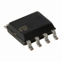
M41T82RM6F STMicroelectronics, M41T82RM6F Datasheet - Page 15

M41T82RM6F
Manufacturer Part Number
M41T82RM6F
Description
IC RTC SERIAL W/BATT SW 8-SOIC
Manufacturer
STMicroelectronics
Type
Clock/Calendar/Alarmr
Datasheet
1.M41T82SM6F.pdf
(61 pages)
Specifications of M41T82RM6F
Memory Size
32B
Time Format
HH:MM:SS:hh (24 hr)
Date Format
YY-MM-DD-dd
Interface
I²C, 2-Wire Serial
Voltage - Supply
2.7 V ~ 5.5 V
Operating Temperature
-40°C ~ 85°C
Mounting Type
Surface Mount
Package / Case
8-SOIC (3.9mm Width)
Lead Free Status / RoHS Status
Lead free / RoHS Compliant
Other names
497-8279-2
M41T82RM6F
M41T82RM6F
Available stocks
Company
Part Number
Manufacturer
Quantity
Price
Company:
Part Number:
M41T82RM6F
Manufacturer:
ST
Quantity:
15 734
M41T82-M41T83
2.2
Read mode
In this mode the master reads the M41T8x slave after setting the slave address (see
Figure 13 on page
acknowledge bit, the word address 'An' is written to the on-chip address pointer. Next the
START condition and slave address are repeated followed by the READ mode control bit
(R/W = 1). At this point the master transmitter becomes the master receiver. The data byte
which was addressed will be transmitted and the master receiver will send an acknowledge
bit to the slave transmitter. The address pointer is only incremented on reception of an
acknowledge clock. The M41T8x slave transmitter will now place the data byte at address
An+1 on the bus, the master receiver reads and acknowledges the new byte and the
address pointer is incremented to An+2.
This cycle of reading consecutive addresses will continue until the master receiver sends a
STOP condition to the slave transmitter. Most of the registers and memory locations are
accessed directly, but the RTC counters are accessed via a set of buffer/transfer registers at
addresses 00h to 07h. The counters are not directly read nor written. Instead, at the start of
a read or write cycle, the counters are copied into the eight buffer/transfer registers so that
the user can read them out sequentially, receiving a coherent set of data, copied from the
same instant in time.
An alternate READ mode may also be implemented whereby the master reads the M41T8x
slave without first writing to the (volatile) address pointer. The first address that is read is the
last one stored in the pointer (see
Figure 12. Slave address location
16). Following the WRITE mode control bit (R/W = 0) and the
START
Doc ID 12578 Rev 12
Figure 14 on page
1
1
SLAVE ADDRESS
0
1
0
0
16).
0
R/W
A
Operation
AI00602
15/61


