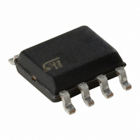
M41T56M6E STMicroelectronics, M41T56M6E Datasheet - Page 14

M41T56M6E
Manufacturer Part Number
M41T56M6E
Description
IC SRAM SRL TIMEKPR 512BIT 8SOIC
Manufacturer
STMicroelectronics
Type
Clock/Calendar/NVSRAMr
Specifications of M41T56M6E
Memory Size
56B
Time Format
HH:MM:SS (24 hr)
Date Format
YY-MM-DD-dd
Interface
I²C, 2-Wire Serial
Voltage - Supply
4.5 V ~ 5.5 V
Operating Temperature
-40°C ~ 85°C
Mounting Type
Surface Mount
Package / Case
8-SOIC (3.9mm Width)
Function
Clock/Calendar
Rtc Memory Size
64 Byte
Supply Voltage (max)
5.5 V
Supply Voltage (min)
4.5 V
Maximum Operating Temperature
+ 85 C
Minimum Operating Temperature
- 40 C
Mounting Style
SMD/SMT
Rtc Bus Interface
Serial (2-Wire, I2C)
Nvram Features
RTC, Internal Battery, XTAL
Interface Type
I2C, Serial, 2-Wire
Supply Voltage Range
4.5V To 5.5V
Memory Case Style
SOIC
No. Of Pins
8
Rohs Compliant
Yes
Lead Free Status / RoHS Status
Contains lead / RoHS non-compliant
Other names
497-2818-5
M41T56M6
M41T56M6
Available stocks
Company
Part Number
Manufacturer
Quantity
Price
Part Number:
M41T56M6E
Manufacturer:
ST
Quantity:
20 000
M41T56
Output Driver Pin
When the FT Bit is not set, the FT/OUT pin be-
comes an output driver that reflects the contents of
D7 of the Control Register. In other words, when
D6 of location 7 is a '0' and D7 of location 7 is a '0'
and then the FT/OUT pin will be driven low.
Note: The FT/OUT pin is open drain which re-
quires an external pull-up resistor.
MAXIMUM RATING
Stressing the device above the rating listed in the
“Absolute Maximum Ratings” table may cause
permanent damage to the device. These are
stress ratings only and operation of the device at
these or any other conditions above those indicat-
ed in the Operating sections of this specification is
Table 4. Absolute Maximum Ratings
Note: 1. For SO package, standard (SnPb) lead finish: Reflow at peak temperature of 225°C (total thermal budget not to exceed 180°C for
14/24
T
Symbol
2. For SO package, Lead-free (Pb-free) lead finish: Reflow at peak temperature of 260°C (total thermal budget not to exceed 245°C
SLD
T
V
V
P
between 90 to 150 seconds).
for greater than 30 seconds).
CAUTION: Negative undershoots below –0.3V are not allowed on any pin while in the Battery Back-up mode.
CAUTION: Do NOT wave solder SOIC to avoid damaging SNAPHAT sockets.
T
STG
I
CC
O
IO
A
D
(1,2)
Ambient Operating Temperature
Storage Temperature (V
Lead Solder Temperature for 10 seconds
Input or Output Voltages
Supply Voltage
Output Current
Power Dissipation
CC
Parameter
Off, Oscillator Off)
Initial Power-on Defaults
Upon initial application of power to the device, the
FT Bit will be set to a '0' and the OUT Bit will be set
to a '1.' All other Register bits will initially power-on
in a random state.
not implied. Exposure to Absolute Maximum Rat-
ing conditions for extended periods may affect de-
vice
STMicroelectronics SURE Program and other rel-
evant quality documents.
SNAPHAT
reliability.
SOIC
Refer
–55 to 125
–40 to 85
–40 to 85
–0.3 to 7
–0.3 to 7
Value
0.25
260
20
also
to
Unit
mA
°C
°C
°C
W
V
V
the


