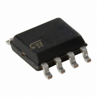
M41T56M6E STMicroelectronics, M41T56M6E Datasheet - Page 6

M41T56M6E
Manufacturer Part Number
M41T56M6E
Description
IC SRAM SRL TIMEKPR 512BIT 8SOIC
Manufacturer
STMicroelectronics
Type
Clock/Calendar/NVSRAMr
Specifications of M41T56M6E
Memory Size
56B
Time Format
HH:MM:SS (24 hr)
Date Format
YY-MM-DD-dd
Interface
I²C, 2-Wire Serial
Voltage - Supply
4.5 V ~ 5.5 V
Operating Temperature
-40°C ~ 85°C
Mounting Type
Surface Mount
Package / Case
8-SOIC (3.9mm Width)
Function
Clock/Calendar
Rtc Memory Size
64 Byte
Supply Voltage (max)
5.5 V
Supply Voltage (min)
4.5 V
Maximum Operating Temperature
+ 85 C
Minimum Operating Temperature
- 40 C
Mounting Style
SMD/SMT
Rtc Bus Interface
Serial (2-Wire, I2C)
Nvram Features
RTC, Internal Battery, XTAL
Interface Type
I2C, Serial, 2-Wire
Supply Voltage Range
4.5V To 5.5V
Memory Case Style
SOIC
No. Of Pins
8
Rohs Compliant
Yes
Lead Free Status / RoHS Status
Contains lead / RoHS non-compliant
Other names
497-2818-5
M41T56M6
M41T56M6
Available stocks
Company
Part Number
Manufacturer
Quantity
Price
Part Number:
M41T56M6E
Manufacturer:
ST
Quantity:
20 000
M41T56
OPERATION
The M41T56 clock operates as a slave device on
the serial bus. Access is obtained by implementing
a start condition followed by the correct slave ad-
dress (D0h). The 64 bytes contained in the device
can then be accessed sequentially in the following
order:
1. Seconds Register
2. Minutes Register
3. Century/Hours Register
4. Day Register
5. Date Register
6. Month Register
7. Years Register
8. Control Register
9 to 64.RAM
The clock continually monitors V
tolerance condition. Should V
the device terminates an access in progress and
resets the device address counter. Inputs to the
device will not be recognized at this time to pre-
vent erroneous data from being written to the de-
vice from an out of tolerance system. When V
falls below V
es over to the battery and powers down into an ul-
tra low current mode of operation to conserve
battery life. Upon power-up, the device switches
from battery to V
when V
2-Wire Bus Characteristics
This bus is intended for communication between
different ICs. It consists of two lines: one bi-direc-
tional for data signals (SDA) and one for clock sig-
nals (SCL). Both the SDA and the SCL lines must
be connected to a positive supply voltage via a
pull-up resistor.
The following protocol has been defined:
–
–
–
Accordingly, the following bus conditions have
been defined:
6/24
Data transfer may be initiated only when the
bus is not busy.
During data transfer, the data line must remain
stable whenever the clock line is High.
Changes in the data line while the clock line is
High will be interpreted as control signals.
CC
goes above V
BAT
, the device automatically switch-
CC
at V
BAT
PFD
and recognizes inputs
volts.
CC
CC
fall below V
for an out of
PFD
CC
,
Bus not busy. Both data and clock lines remain
High.
Start data transfer. A change in the state of the
data line, from High to Low, while the clock is High,
defines the START condition.
Stop data transfer. A change in the state of the
data line, from Low to High, while the clock is High,
defines the STOP condition.
Data valid. The state of the data line represents
valid data when after a start condition, the data line
is stable for the duration of the High period of the
clock signal. The data on the line may be changed
during the Low period of the clock signal. There is
one
Each data transfer is initiated with a start condition
and terminated with a stop condition. The number
of data bytes transferred between the start and
stop conditions is not limited. The information is
transmitted byte-wide and each receiver acknowl-
edges with a ninth bit.
By definition, a device that gives out a message is
called “transmitter,” the receiving device that gets
the message is called “receiver.” The device that
controls the message is called “master.” The de-
vices that are controlled by the master are called
“slaves.”
Acknowledge. Each byte of eight bits is followed
by one Acknowledge Bit. This Acknowledge Bit is
a low level put on the bus by the receiver, whereas
the master generates an extra acknowledge relat-
ed clock pulse.
A slave receiver which is addressed is obliged to
generate an acknowledge after the reception of
each byte. Also, a master receiver must generate
an acknowledge after the reception of each byte
that has been clocked out of the slave transmitter.
The device that acknowledges has to pull down
the SDA line during the acknowledge clock pulse
in such a way that the SDA line is a stable Low dur-
ing the High period of the acknowledge related
clock pulse. Of course, setup and hold times must
be taken into account. A master receiver must sig-
nal an end-of-data to the slave transmitter by not
generating an acknowledge on the last byte that
has been clocked out of the slave. In this case, the
transmitter must leave the data line High to enable
the master to generate the STOP condition.
clock
pulse
per
bit
of
data.


