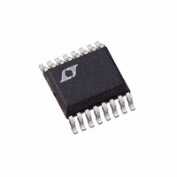
LTC2440IGN#TRPBF Linear Technology, LTC2440IGN#TRPBF Datasheet - Page 15

LTC2440IGN#TRPBF
Manufacturer Part Number
LTC2440IGN#TRPBF
Description
IC ADC DIFFER 24-BIT HS 16-SSOP
Manufacturer
Linear Technology
Datasheet
1.LTC2440CGN.pdf
(28 pages)
Specifications of LTC2440IGN#TRPBF
Number Of Bits
24
Sampling Rate (per Second)
3.5k
Data Interface
MICROWIRE™, Serial, SPI™
Number Of Converters
2
Power Dissipation (max)
40mW
Voltage Supply Source
Single Supply
Operating Temperature
-40°C ~ 85°C
Mounting Type
Surface Mount
Package / Case
16-SSOP (0.150", 3.90mm Width)
Lead Free Status / RoHS Status
Lead free / RoHS Compliant
Available stocks
Company
Part Number
Manufacturer
Quantity
Price
APPLICATIONS INFORMATION
EOC = 1 (BUSY = 1) while a conversion is in progress
and EOC = 0 (BUSY = 0) if the device is in the sleep state.
Independent of CS, the device automatically enters the low
power sleep state once the conversion is complete.
When the device is in the sleep state (EOC = 0), its con-
version result is held in an internal static shift register.
The device remains in the sleep state until the fi rst rising
edge of SCK is seen. Data is shifted out the SDO pin on
each falling edge of SCK. This enables external circuitry
to latch the output on the rising edge of SCK. EOC can be
latched on the fi rst rising edge of SCK and the last bit of
the conversion result can be latched on the 32nd rising
edge of SCK. On the 32nd falling edge of SCK, the device
begins a new conversion. SDO goes HIGH (EOC = 1) and
BUSY goes HIGH indicating a conversion is in progress.
At the conclusion of the data cycle, CS may remain LOW
and EOC monitored as an end-of-conversion interrupt.
Alternatively, CS may be driven HIGH setting SDO to Hi-Z
and BUSY monitored for the completion of a conversion.
As described above, CS may be pulled LOW at any time in
order to monitor the conversion status on the SDO pin.
(EXTERNAL)
BUSY
SDO
SCK
CS
CONVERSION
Hi-Z
TEST EOC
TEST EOC
SLEEP
Hi-Z
BIT 31
Figure 5. External Serial Clock, Single Cycle Operation
EOC
ANALOG INPUT RANGE
BIT 30
REFERENCE VOLTAGE
–0.5V
REF
0.1V TO V
TO 0.5V
BIT 29
SIG
1μF
4.5V TO 5.5V
REF
CC
1, 8, 9, 16
BIT 28
MSB
2
3
4
5
6
V
REF
REF
IN
IN
GND
CC
+
–
LTC2440
+
–
Typically, CS remains LOW during the data output state.
However, the data output state may be aborted by pulling
CS HIGH anytime between the fi fth falling edge (SDI must
be properly loaded each cycle) and the 32nd falling edge
of SCK, see Figure 6. On the rising edge of CS, the device
aborts the data output state and immediately initiates a
new conversion. This is useful for systems not requiring
all 32-bits of output data, aborting an invalid conversion
cycle or synchronizing the start of a conversion.
External Serial Clock, 2-Wire I/O
This timing mode utilizes a 2-wire serial I/O interface.
The conversion result is shifted out of the device by an
externally generated serial clock (SCK) signal, see Figure
7. CS may be permanently tied to ground, simplifying the
user interface or isolation barrier. The external serial clock
mode is selected by tying EXT LOW.
Since CS is tied LOW, the end-of-conversion (EOC) can
be continuously monitored at the SDO pin during the
convert and sleep states. Conversely, BUSY (Pin 15) may
be used to monitor the status of the conversion cycle.
EOC or BUSY may be used as an interrupt to an external
BIT 27
BUSY
SDO
SCK
EXT
DATA OUTPUT
SDI
CS
f
O
15
14
13
12
11
7
10
BIT 26
3-WIRE
SPI INTERFACE
V
CC
= EXTERNAL OSCILLATOR
= INTERNAL OSCILLATOR
200nV NOISE, 50/60Hz REJECTION
10-SPEED/RESOLUTION PROGRAMMABLE
2μV NOISE, 880Hz OUTPUT RATE
BIT 5
LSB
SUB LSB
BIT 0
LTC2440
CONVERSION
Hi-Z
TEST EOC
15
2440 F05
2440fd


