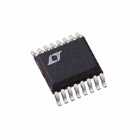
LTC2440IGN#TRPBF Linear Technology, LTC2440IGN#TRPBF Datasheet - Page 8

LTC2440IGN#TRPBF
Manufacturer Part Number
LTC2440IGN#TRPBF
Description
IC ADC DIFFER 24-BIT HS 16-SSOP
Manufacturer
Linear Technology
Datasheet
1.LTC2440CGN.pdf
(28 pages)
Specifications of LTC2440IGN#TRPBF
Number Of Bits
24
Sampling Rate (per Second)
3.5k
Data Interface
MICROWIRE™, Serial, SPI™
Number Of Converters
2
Power Dissipation (max)
40mW
Voltage Supply Source
Single Supply
Operating Temperature
-40°C ~ 85°C
Mounting Type
Surface Mount
Package / Case
16-SSOP (0.150", 3.90mm Width)
Lead Free Status / RoHS Status
Lead free / RoHS Compliant
Available stocks
Company
Part Number
Manufacturer
Quantity
Price
PIN FUNCTIONS
LTC2440
GND (Pins 1, 8, 9, 16): Ground. Multiple ground pins
internally connected for optimum ground current fl ow and
V
plane through a low impedance connection. All four pins
must be connected to ground for proper operation.
V
(Pin 1) with a 10μF tantalum capacitor in parallel with 0.1μF
ceramic capacitor as close to the part as possible.
REF
The voltage on these pins can have any value between
GND and V
is maintained more positive than the reference negative
input, REF
IN
voltage on these pins can have any value between GND
– 0.3V and V
bipolar input range (V
• (V
converter produces unique overrange and underrange
output codes.
SDI (Pin 7): Serial Data Input. This pin is used to select
the speed/resolution of the converter. If SDI is grounded
(pin compatible with LTC2410) the device outputs data at
880Hz with 21 bits effective resolution. By tying SDI HIGH,
the converter enters the ultralow noise mode (200nV
with simultaneous 50/60Hz rejection at 6.9Hz output
rate. SDI may be driven logic HIGH or LOW anytime dur-
ing the conversion or sleep state in order to change the
speed/resolution. The conversion immediately following
the data output cycle will be valid and performed at the
newly selected output rate/resolution. SDI may also be
programmed by a serial input data stream under control of
SCK during the data output cycle. One of ten speed/resolu-
tion ranges (from 6.9Hz/200nV
may be selected. The fi rst conversion following a new
selection is valid and performed at the newly selected
speed/resolution.
EXT (Pin 10): Internal/External SCK Selection Pin. This pin
is used to select internal or external SCK for outputting
data. If EXT is tied low (pin compatible with the LTC2410),
the device is in the external SCK mode and data is shifted
out the device under the control of a user applied serial
clock. If EXT is tied high, the internal serial clock mode
8
CC
CC
+
decoupling. Connect each one of these pins to a ground
+
(Pin 5), IN
REF
(Pin 2): Positive Supply Voltage. Bypass to GND
(Pin 3), REF
) to 0.5 • (V
CC
–
, by at least 0.1V.
as long as the reference positive input, REF
CC
–
+ 0.3V. Within these limits the converter
(Pin 6): Differential Analog Input. The
–
(Pin 4): Differential Reference Input.
REF
IN
). Outside this input range the
= IN
+
– IN
RMS
–
) extends from –0.5
to 3.5kHz/21μV
RMS
RMS
+
)
)
,
is selected. The device generates its own SCK signal and
outputs this on the SCK pin. A framing signal BUSY (Pin 15)
goes low indicating data is being output.
CS (Pin 11): Active LOW Digital Input. A LOW on this pin
enables the SDO digital output and wakes up the ADC.
Following each conversion the ADC automatically enters
the Sleep mode and remains in this low power state as
long as CS is HIGH. A LOW-to-HIGH transition on CS
during the Data Output transfer aborts the data transfer
and starts a new conversion.
SDO (Pin 12): Three-State Digital Output. During the Data
Output period, this pin is used as serial data output. When
the chip select CS is HIGH (CS = V
high impedance state. During the Conversion and Sleep
periods, this pin is used as the conversion status output. The
conversion status can be observed by pulling CS LOW.
SCK (Pin 13): Bidirectional Digital Clock Pin. In Internal
Serial Clock Operation mode, SCK is used as digital output
for the internal serial interface clock during the Data Output
period. In External Serial Clock Operation mode, SCK is used
as digital input for the external serial interface clock during
the Data Output period. The Serial Clock Operation mode is
determined by the logic level applied to the EXT pin.
f
trols the internal conversion clock. When f
V
at 9MHz. The conversion rate is determined by the selected
OSR such that t
(t
32768). The fi rst null is located at 8/t
256 and 55Hz (simultaneous 50/60Hz) at OSR = 32768.
When f
kHz), the conversion time becomes t
170)/f
BUSY (Pin 15): Conversion in Progress Indicator. For
compatibility with the LTC2410, this pin should not be
tied to ground. This pin is HIGH while the conversion
is in progress and goes LOW indicating the conversion
is complete and data is ready. It remains low during the
sleep and data output states. At the conclusion of the data
output state, it goes HIGH indicating a new conversion
has begun.
O
CC
CONV
(Pin 14): Frequency Control Pin. Digital input that con-
or GND, the converter uses its internal oscillator running
EOSC
= 1.137ms at OSR = 256, t
O
is driven by an oscillator with frequency f
(in ms) and the fi rst null remains 8/t
CONV
(in ms) = (40 • OSR + 170)/9000
CONV
CC
) the SDO pin is in a
CONV
CONV
= 146ms at OSR =
O
, 7kHz at OSR =
is connected to
= (40 • OSR +
CONV
EOSC
2440fd
.
(in


