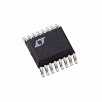
LTC2440IGN#TRPBF Linear Technology, LTC2440IGN#TRPBF Datasheet - Page 24

LTC2440IGN#TRPBF
Manufacturer Part Number
LTC2440IGN#TRPBF
Description
IC ADC DIFFER 24-BIT HS 16-SSOP
Manufacturer
Linear Technology
Datasheet
1.LTC2440CGN.pdf
(28 pages)
Specifications of LTC2440IGN#TRPBF
Number Of Bits
24
Sampling Rate (per Second)
3.5k
Data Interface
MICROWIRE™, Serial, SPI™
Number Of Converters
2
Power Dissipation (max)
40mW
Voltage Supply Source
Single Supply
Operating Temperature
-40°C ~ 85°C
Mounting Type
Surface Mount
Package / Case
16-SSOP (0.150", 3.90mm Width)
Lead Free Status / RoHS Status
Lead free / RoHS Compliant
Available stocks
Company
Part Number
Manufacturer
Quantity
Price
LTC2440
APPLICATIONS INFORMATION
fastest expected input signal. Figure 20 shows the large
signal response of the circuit in Figure 19.
3. Measure noise performance of the complete circuit. A
good technique is to build one amplifi er for each input,
even if only one will be used in the end application. Bias
both amplifi er outputs to midscale, with the inputs tied
together. Verify that the noise is as expected, taking into
account the bandwidth of the LTC2440 inputs for the OSR
being used, the amplifi er’s broadband voltage noise and
1/f corner (if any) and any additional noise due to the
amplifi er’s current noise and source resistance.
24
Figure 20. Large Signal Input Settling Time Indicates
Completed Settling with Selected Load Capacitance.
IN–
IN+
Figure 19. Buffering the LTC2440 from High Impedance Sources Using a Chopper Amplifi er
+
+
–
–
1
1
/
/
2
2
100μs/DIV
LTC2051HV
LTC2051HV
C1
C4
0.01μF
0.01μF
10Ω
10Ω
2440 F20
R1
R2
R4
R5
5k
5k
8-12V
C2
C5
LT1236-5
1μF
1μF
For more information on testing high linearity ADCs, refer
to Linear Technology Design Solutions 11.
Input Bandwidth and Frequency Rejection
The combined effect of the internal SINC
the digital and analog autocalibration circuits determines
the LTC2440 input bandwidth and rejection characteristics.
The digital fi lter’s response can be adjusted by setting the
oversample ratio (OSR) through the SPI interface or by
supplying an external conversion clock to the f
Figure 21. Dynamic Input Current is Attenuated by Load
Capacitance and Completely Settled Before the Next Conversion
Sample Resulting in No Reduction in Performance.
C2, C5 TAIYO YUDEN JMK107BJ105MA
4.7μF
0.1μF
1, 8, 9, 16
4
5
6
V
REF
REF
IN
IN
5ns/DIV
CC
+
–
LTC2440
+
–
BUSY
0.01μF
SDO
SCK
EXT
SDI
CS
f
O
15
14
13
12
11
7
10
2440 F19
2440 F21
4
10μF
5V
digital fi lter and
O
pin.
2440fd


