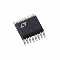
LTC2440IGN#TRPBF Linear Technology, LTC2440IGN#TRPBF Datasheet - Page 17

LTC2440IGN#TRPBF
Manufacturer Part Number
LTC2440IGN#TRPBF
Description
IC ADC DIFFER 24-BIT HS 16-SSOP
Manufacturer
Linear Technology
Datasheet
1.LTC2440CGN.pdf
(28 pages)
Specifications of LTC2440IGN#TRPBF
Number Of Bits
24
Sampling Rate (per Second)
3.5k
Data Interface
MICROWIRE™, Serial, SPI™
Number Of Converters
2
Power Dissipation (max)
40mW
Voltage Supply Source
Single Supply
Operating Temperature
-40°C ~ 85°C
Mounting Type
Surface Mount
Package / Case
16-SSOP (0.150", 3.90mm Width)
Lead Free Status / RoHS Status
Lead free / RoHS Compliant
Available stocks
Company
Part Number
Manufacturer
Quantity
Price
APPLICATIONS INFORMATION
controller indicating the conversion result is ready. EOC
= 1 (BUSY = 1) while the conversion is in progress and
EOC = 0 (BUSY = 0) once the conversion enters the low
power sleep state. On the falling edge of EOC/BUSY, the
conversion result is loaded into an internal static shift
register. The device remains in the sleep state until the
fi rst rising edge of SCK. Data is shifted out the SDO pin
on each falling edge of SCK enabling external circuitry to
latch data on the rising edge of SCK. EOC can be latched
on the fi rst rising edge of SCK. On the 32nd falling edge
of SCK, SDO and BUSY go HIGH (EOC = 1) indicating a
new conversion has begun.
Internal Serial Clock, Single Cycle Operation
This timing mode uses an internal serial clock to shift out
the conversion result and a CS signal to monitor and control
the state of the conversion cycle, see Figure 8.
In order to select the internal serial clock timing mode,
the EXT pin must be tied HIGH.
The serial data output pin (SDO) is Hi-Z as long as CS is
HIGH. At any time during the conversion cycle, CS may be
pulled LOW in order to monitor the state of the converter.
(INTERNAL)
BUSY
SDO
SCK
CS
CONVERSION
Hi-Z
TEST EOC
SLEEP
Hi-Z
<t
EOCtest
BIT 31
EOC
Figure 8. Internal Serial Clock, Single Cycle Operation
BIT 30
ANALOG INPUT RANGE
REFERENCE VOLTAGE
–0.5V
REF
0.1V TO V
TO 0.5V
BIT 29
SIG
1μF
4.5V TO 5.5V
REF
CC
1, 8, 9, 16
BIT 28
MSB
2
3
4
5
6
V
REF
REF
IN
IN
GND
CC
+
–
LTC2440
+
–
BIT 27
Once CS is pulled LOW, SCK goes LOW and EOC is output
to the SDO pin. EOC = 1 while a conversion is in progress
and EOC = 0 if the device is in the sleep state. Alterna-
tively, BUSY (Pin 15) may be used to monitor the status
of the conversion in progress. BUSY is HIGH during the
conversion and goes LOW at the conclusion. It remains
LOW until the result is read from the device.
When testing EOC, if the conversion is complete (EOC =
0), the device will exit the sleep state and enter the data
output state if CS remains LOW. In order to prevent the
device from exiting the low power sleep state, CS must
be pulled HIGH before the fi rst rising edge of SCK. In the
internal SCK timing mode, SCK goes HIGH and the device
begins outputting data at time t
of CS (if EOC = 0) or t
LOW during the falling edge of EOC). The value of t
is 500ns. If CS is pulled HIGH before time tE
device remains in the sleep state. The conversion result
is held in the internal static shift register.
If CS remains LOW longer than t
edge of SCK will occur and the conversion result is serially
shifted out of the SDO pin. The data output cycle begins
BUSY
SDO
SCK
EXT
SDI
DATA OUTPUT
CS
f
O
15
14
13
12
11
7
10
BIT 26
V
CC
3-WIRE
SPI INTERFACE
V
CC
= EXTERNAL OSCILLATOR
= INTERNAL OSCILLATOR
200nV NOISE, 50/60Hz REJECTION
10-SPEED/RESOLUTION PROGRAMMABLE
2μV NOISE, 880Hz OUTPUT RATE
EOCtest
LSB
BIT 5
24
after EOC goes LOW (if CS is
EOCtest
EOCtest
BIT 0
after the falling edge
LTC2440
, the fi rst rising
CONVERSION
Hi-Z
OCtest
TEST EOC
17
EOCtest
, the
2440 F08
Hi-Z
2440fd


