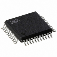
ADC1006S055H/C1,51 NXP Semiconductors, ADC1006S055H/C1,51 Datasheet - Page 6

ADC1006S055H/C1,51
Manufacturer Part Number
ADC1006S055H/C1,51
Description
IC ADC 10BIT PAR 55MHZ 44-QFP
Manufacturer
NXP Semiconductors
Datasheet
1.ADC1006S055HC155.pdf
(31 pages)
Specifications of ADC1006S055H/C1,51
Number Of Bits
10
Sampling Rate (per Second)
55M
Data Interface
Parallel
Number Of Converters
1
Power Dissipation (max)
660mW
Voltage Supply Source
Analog and Digital
Operating Temperature
-40°C ~ 85°C
Mounting Type
Surface Mount
Package / Case
44-MQFP, 44-PQFP
Lead Free Status / RoHS Status
Lead free / RoHS Compliant
Other names
935286763518
ADC1006S055H/C1-T
ADC1006S055H/C1-T
ADC1006S055H/C1-T
ADC1006S055H/C1-T
Available stocks
Company
Part Number
Manufacturer
Quantity
Price
Company:
Part Number:
ADC1006S055H/C1,51
Manufacturer:
IDT, Integrated Device Technology Inc
Quantity:
10 000
NXP Semiconductors
9. Thermal characteristics
10. Characteristics
Table 6.
V
V
V
and V
ADC1006S055_070_2
Product data sheet
Symbol
Supplies
V
V
V
I
I
I
P
Inputs
CLK and CLKN (referenced to DGND)
V
CCA
CCD
CCO
CCA
CCO
I(IN)(p-p)
CCA
CCD
CCO
tot
IL
= V2 to V44, V3 to V4 and V41 to V40 = 4.75 V to 5.25 V; V
= V33 to V34 = 3.0 V to 3.6 V; AGND and DGND shorted together; T
CCO
= 3.3 V, T
V
Characteristics
I(INN)(p-p)
Parameter
analog supply
voltage
digital supply
voltage
output supply
voltage
analog supply
current
digital supply
current
output supply
current
total power
dissipation
LOW-level input
voltage
amb
= 1.9 V; V
= 25 C and C
Table 4.
In accordance with the Absolute Maximum Rating System (IEC 60134).
[1]
Table 5.
Symbol
V
I
T
T
T
Symbol
R
O
stg
amb
j
i(clk)(p-p)
th(j-a)
The supply voltages V
the supply voltage differences V
VREF
Conditions
f
f
f
PECL mode; V
TTL mode
clk
clk
clk
= V
Limiting values
Thermal characteristics
= 20 MHz; f
= 55 MHz; f
= 55 MHz; f
L
Parameter
thermal resistance from junction to
ambient
Parameter
peak-to-peak clock input
voltage
output current
storage temperature
ambient temperature
junction temperature
[2]
CCA3
= 10 pF; unless otherwise specified.
1.75 V; V
CCA
i
i
i
CCD
Rev. 02 — 12 August 2008
= 400 kHz
= 20 MHz
= 20 MHz
, V
= 5 V
…continued
CCD
I(cm)
and V
CC
= V
are respected.
CCA3
CCO
Test
I
I
I
I
I
C
CCD
may have any value between 0.3 V and +7.0 V provided that
Conditions
differential clock
drive at pins
35 and 36
= V37 to V38 and V15 to V17 = 4.75 V to 5.25 V;
[1]
1.6 V; typical values measured at V
Single 10 bits ADC, up to 55 MHz or 70 MHz
Min
4.75
4.75
3.0
-
-
-
-
-
3.19
0
amb
= 40 C to +85 C;
ADC1006S055/070
Condition
in free air
Typ
5.0
5.0
3.3
78
27
3
9.5
550
-
-
Min
-
-
-
55
40
Max
5.25
5.25
3.6
87
30
4
12
660
3.52
0.8
Max
V
10
+150
+85
150
Value
75
© NXP B.V. 2008. All rights reserved.
CCD
CCA
= V
CCD
Unit
V
mA
Unit
K/W
C
C
C
Unit
V
V
V
mA
mA
mA
mA
mW
V
V
6 of 31
= 5 V


