HI7188IN Intersil, HI7188IN Datasheet - Page 18
HI7188IN
Manufacturer Part Number
HI7188IN
Description
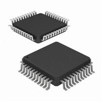
CONV A/D 16BIT 8:1 MUX 44-MQFP
Manufacturer
Intersil
Datasheet
1.HI7188IN.pdf
(24 pages)
Specifications of HI7188IN
Number Of Bits
16
Sampling Rate (per Second)
240
Data Interface
QSPI™, Serial, SPI™
Number Of Converters
1
Power Dissipation (max)
50mW
Voltage Supply Source
Analog and Digital, Dual ±
Operating Temperature
-40°C ~ 85°C
Mounting Type
Surface Mount
Package / Case
44-QFP
Lead Free Status / RoHS Status
Contains lead / RoHS non-compliant
Available stocks
Company
Part Number
Manufacturer
Quantity
Price


Serial Interface
The HI7188 has a flexible, synchronous serial
communication port to allow easy interfacing to most
industry standard microcontrollers and microprocessors.
The serial I/O is compatible with most synchronous transfer
formats, including both the Motorola 6805/11, SPI and Intel
8051 SSR protocols. The interface supports 2-wire transfers
of reading and writing on a single bidirectional line (SDIO) or
3-wire transfers of writing on SDIO and reading on the SDO
line.
The Interface allows read/write access to the Control
Register, Channel Configuration Registers, and Calibration
RAMs. The interface allows read only access to the data
RAM (refer to Table 7). The interface is byte organized with
each register byte having a specific address. Single or
multiple byte transfers are supported. In addition, the
interface allows flexibility as to the byte and bit access order.
That is, the user can specify MSB/LSB first bit positioning
and can access bytes in ascending/descending order from
any byte position.
Serial Interface Clock
The HI7188 supports two serial interface clock (SCLK)
modes for all interface timing. This allows the greatest
flexibility for different types of systems where the HI7188 can
act either as master in the system (it provides the serial
interface clock) or as slave (an external clock is provided to
the HI7188). These two modes are defined as self clocking
and external clocking respectively. Regardless of the
clocking mode selected, all data is registered into
the HI7188 on the rising edge of the SCLK while all data is
driven out on the falling edge of SCLK. The HI7188 interface
is designed to work with clock stalling in either high or low
state. The clock mode is determined by the logic level applied
to the MODE pin.
Synchronous Self Clocking
The device in a self-clocking scheme if the MODE pin is
high. This defines the SCLK pin as an output which provides
the serial clock signal used for the transfer of all data to and
from the HI7188. This self-clocking mode can be used with
processors which allow an external device to clock their
serial port. The frequency of SCLK is one eighth of the
external crystal connected between the OSC
pins. The HI7188 is designed for a 3.6864MHz crystal which
sets SCLK to 460.8kHz.
Synchronous External Clocking
The HI7188 is in a external clocking scheme if the MODE pin is
low. This defines the SCLK pin as an input and an external
clock must be provided to the SCLK pin. This external clocking
mode is designed for direct interface to systems which provide
a serial clock output which is synchronized to the serial data
output. The maximum frequency of the external SCLK is 5MHz.
18
1
and OSC
2
HI7188
Burst RAM Access
The Data RAM, System Offset calibration RAM, System
Positive Full Scale Calibration RAM and System Negative Full
Scale Calibration RAM can only be accessed in a continuous
RAM “Burst”. RAM burst transfers are special instructions that
perform a continuous data transfer for all bits of that RAM.
That is, individual bytes of any RAM cannot be accessed
without reading all of the bytes. See Table 7. Each transfer
occurs such that the first word transferred corresponds to the
first logical channel converted as specified in the Channel
Configuration Register (CCR). The first byte transferred for
each word is controlled by the RB bit of the instruction byte
and the bit position is determined by the Control Register
(CR) MSB/LSB bit. The number of words transferred is
specified by the CR bits that describe the number of logical
channels being converted as well as the size of the
destination RAM. This transfer mode reduces the overhead of
multiple IR writes as compared to individual byte access. The
following two examples are useful in understanding the RAM
burst transfer instructions.
Example 1. The physical channel conversion order as
specified by the CCRs is 8, 2, 3, 4, 5, 6, 1, 7. The HI7188 is
setup via the Control Register to convert 8 logical channels.
The IR byte written is 0xx11100 (read the data RAM). The
following occurs: After completing the IR write, 16 bytes of
data will be transferred from the HI7188. The first byte
transferred will be the most significant byte of the physical
channel 8 conversion results. The second byte will be the
least significant byte of the physical channel 8 conversion
results. This pattern of most significant byte followed by least
significant byte will repeat, in order for physical channels 2,
3, 4, 5, 6, 1, 7.
Example 2. The physical channel conversion order as
specified by the CCRs is 8, 2, 3, 4, 5, 6, 1, 7. The HI7188 is
setup via the Control Register to convert only 3 logical
channels. The IR byte written is 1xx01101 (write the offset
RAM). The following occurs: After completing the IR write, 9
bytes of data will be written to the offset RAM (recall that the
Offset Calibration register is 3 bytes wide). The first byte is
the least significant byte used for offset calibration of
physical channel 8. The second byte will be the middle byte
used for offset calibration of physical channel 8. The third
byte will be the most significant byte used for offset
calibration of physical channel 8. This pattern of least
significant byte to most significant byte will repeat for all
logical channels converted in the logical channel order as
described above. For example, the last byte transferred will
be the most significant byte of physical channel 3 used for
offset calibration.
NOTE: When the user accesses the calibration RAMs, via the
Serial Interface, the conversion process stops, resetting the
modulator, integrating filter and clearing the EOS interrupt. When the
calibration RAM I/O operation is completed the device automatically
restarts beginning on logical channel 1. The contents of the CR and
CCR are not affected by this I/O.
Related parts for HI7188IN
Image
Part Number
Description
Manufacturer
Datasheet
Request
R

Part Number:
Description:
8-channel, 16-bit, High Precision, Sigma-delta A/d Sub-system
Manufacturer:
Intersil Corporation
Datasheet:
Part Number:
Description:
Intersil Corporation [CMOS Serial Controller Interface]
Manufacturer:
Intersil Corporation
Datasheet:
Part Number:
Description:
Manufacturer:
Intersil Corporation
Datasheet:
Part Number:
Description:
357-036-542-201 CARDEDGE 36POS DL .156 BLK LOPRO
Manufacturer:
Intersil Corporation
Datasheet:
Part Number:
Description:
1024-Word x 4-Bit LSI Static RAM
Manufacturer:
Intersil Corporation
Datasheet:
Part Number:
Description:
General Purpose NPN Transistor Arrays FN341.4
Manufacturer:
Intersil Corporation
Datasheet:
Part Number:
Description:
CMOS 16-Bit Microprocessor
Manufacturer:
Intersil Corporation
Datasheet:
Part Number:
Description:
Manufacturer:
Intersil Corporation
Datasheet:
Part Number:
Description:
Manufacturer:
Intersil Corporation
Datasheet:
Part Number:
Description:
Manufacturer:
Intersil Corporation
Datasheet:
Part Number:
Description:
Manufacturer:
Intersil Corporation
Datasheet:
Part Number:
Description:
CMOS 6-Bit Latch and Decoder Memory Interfaces
Manufacturer:
Intersil Corporation
Datasheet:
Part Number:
Description:
CA3046General Purpose NPN Transistor Arrays
Manufacturer:
Intersil Corporation
Datasheet:
Part Number:
Description:
Manufacturer:
Intersil Corporation
Datasheet:
Part Number:
Description:
TR909 DLC/FLC SLIC with Low Power Standby
Manufacturer:
Intersil Corporation
Datasheet: