HI7188IN Intersil, HI7188IN Datasheet - Page 22
HI7188IN
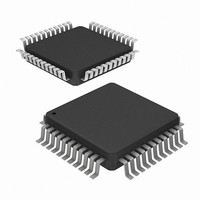
Manufacturer Part Number
HI7188IN
Description
CONV A/D 16BIT 8:1 MUX 44-MQFP
Manufacturer
Intersil
Datasheet
1.HI7188IN.pdf
(24 pages)
Specifications of HI7188IN
Number Of Bits
16
Sampling Rate (per Second)
240
Data Interface
QSPI™, Serial, SPI™
Number Of Converters
1
Power Dissipation (max)
50mW
Voltage Supply Source
Analog and Digital, Dual ±
Operating Temperature
-40°C ~ 85°C
Mounting Type
Surface Mount
Package / Case
44-QFP
Lead Free Status / RoHS Status
Contains lead / RoHS non-compliant
Available stocks
Company
Part Number
Manufacturer
Quantity
Price


CS. Chip Select. This signal is an active low input that allows
more than one device on the same serial communication
lines. The SDO and SDIO will go to a high impedance state
when this signal is high. If driven high during any
communication cycle, that cycle will be suspended until CS
reactivation. Chip select can be tied low in systems that
maintain control of SCLK.
EOS. End Of Scan. Signals the end of a logical channel
scan (all programmed logical channels have been
converted) and data is available for reading. EOS is useful
as an edge or level sensitive interrupt signal to a
microprocessor or microcontroller. EOS low indicates that
new data is available and the Data RAM can be read. EOS
will return high upon completion of a complete Data RAM
read cycle. Please refer to the Data RAM section for details.
CA. Calibration Active. This pin is high if any active logical
channel is in the calibration mode and stays high for the
entire scan period. CA checks only those channels that are
actively being converted on. For example, if the HI7188 is
programmed to convert only two channels and any of the
CCR bytes of the six nonactive channels are in the
calibration mode, CA will NOT go active. The user can
monitor the CA output to determine when all active channels
have completed calibration.
MODE. Mode. This input is used to select between
Synchronous Self Clocking Mode (high) or the Synchronous
External Clocking Mode (low).
RSTI/O. Reset I/O. This active low asynchronous input is
used to reset the serial interface state machine. This reset
only affects the I/O logic and does not affect the Control
Register, Channel Configuration Register or Calibration
RAMs. This effectively aborts any communication cycle
and places the device in a standby mode awaiting the next IR
cycle.
Serial Interface Communication
It is useful to think of the HI7188 interface in terms of
communication cycles. Each communication cycle happens in
2 phases. The first phase is the writing of an instruction byte
while the second phase is the data transfer as described by the
instruction byte. It is important to note that phase 2 of the
communication cycle can be a single byte or a multi-byte
transfer of data including a Burst RAM read/write. It is up to the
user to maintain synchronism with respect to data transfers. If
the system processor “gets lost”, during an I/O operation, the
only way to recover is to reset the Serial Interface via a RSTI/O.
Figure 15 shows both a 2-wire and a 3-wire data transfer.
Instruction Byte Phase
The instruction byte phase initiates a data transfer
sequence. The processor writes an eight bit byte to the
“Instruction Register”, known as the “Instruction Byte”. The
instruction byte informs the HI7188 about the Data cycle
phase activities and includes the following information:
• Read or Write Cycle
• Number of Bytes to be Transferred
• Which Register and Starting Byte to be Accessed
22
HI7188
Data Cycle Phase
In the data cycle phase, data transfer takes place as defined
by the Instruction Register Byte. See Write Operation and
Read Operation sections for detailed descriptions. It is
important to note that phase 2 of the communication cycle
can be a multi-byte transfer of data.
For example, the 4 byte Channel Configuration register can be
read using one multi-byte communication cycle rather than four
single byte communication cycles. After phase 2 is completed
the HI7188 I/O logic enters a standby mode while waiting to
receive a new instruction byte. It is up to the user to maintain
synchronism with respect to data transfers. If the system
processor “gets lost” the only way to recover is to reset the
HI7188.
Serial Interface Format
Several formats are available for reading from and writing to
the HI7188 registers in both the 2-wire and 3-wire protocols.
Please refer to Figure 15. A portion of these formats is
controlled by the CR<2:1> (BD and MSB) bits which control
the byte direction and bit order of a data transfer
respectively. These two bits can be written in any
combination but only the two most useful will be discussed
here. The first combination is to reset both the BD and MSB
bits (BD = 0, MSB = 0). This sets up the interface for
descending byte order and MSB first format. When this
combination is used the user should always write the
instruction register such that the starting byte is the most
significant byte address. For example, read three bytes of
data starting with the most significant byte. The first byte
read will be the most significant in MSB to LSB format. The
next byte will be the next least significant (recall descending
byte order) again in MSB to LSB order. The last byte will be
the next lesser significant byte in MSB to LSB order. THE
ENTIRE WORD WAS READ MSB TO LSB format. The
second combination is to set both the BD and MSB bits to 1.
This sets up the interface for ascending byte order and LSB
first format. When this combination is used the user should
always write the instruction register such that the starting
byte is the least significant byte address. For example, read
three bytes of data starting with the least significant byte.
The first byte read will be the least significant in LSB to MSB
format. The next byte will be the next greater significant
(recall ascending byte order) again in LSB to MSB order.
The last byte will be the next greater significant byte in LSB
to MSB order. THE ENTIRE WORD WAS READ LSB TO
MSB format. After completion of each communication cycle,
The HI7188 interface enters a standby mode while waiting to
receive a new instruction byte.
SDIO
SDO
CS
FIGURE 15. 3-WIRE, 3 BYTE READ TRANSFER
INSTRUCTION
INSTRUCTION
CYCLE
BYTE
BYTE 1
DATA
DATA CYCLE
BYTE 2
DATA
BYTE 3
DATA
Related parts for HI7188IN
Image
Part Number
Description
Manufacturer
Datasheet
Request
R

Part Number:
Description:
8-channel, 16-bit, High Precision, Sigma-delta A/d Sub-system
Manufacturer:
Intersil Corporation
Datasheet:
Part Number:
Description:
Intersil Corporation [CMOS Serial Controller Interface]
Manufacturer:
Intersil Corporation
Datasheet:
Part Number:
Description:
Manufacturer:
Intersil Corporation
Datasheet:
Part Number:
Description:
357-036-542-201 CARDEDGE 36POS DL .156 BLK LOPRO
Manufacturer:
Intersil Corporation
Datasheet:
Part Number:
Description:
1024-Word x 4-Bit LSI Static RAM
Manufacturer:
Intersil Corporation
Datasheet:
Part Number:
Description:
General Purpose NPN Transistor Arrays FN341.4
Manufacturer:
Intersil Corporation
Datasheet:
Part Number:
Description:
CMOS 16-Bit Microprocessor
Manufacturer:
Intersil Corporation
Datasheet:
Part Number:
Description:
Manufacturer:
Intersil Corporation
Datasheet:
Part Number:
Description:
Manufacturer:
Intersil Corporation
Datasheet:
Part Number:
Description:
Manufacturer:
Intersil Corporation
Datasheet:
Part Number:
Description:
Manufacturer:
Intersil Corporation
Datasheet:
Part Number:
Description:
CMOS 6-Bit Latch and Decoder Memory Interfaces
Manufacturer:
Intersil Corporation
Datasheet:
Part Number:
Description:
CA3046General Purpose NPN Transistor Arrays
Manufacturer:
Intersil Corporation
Datasheet:
Part Number:
Description:
Manufacturer:
Intersil Corporation
Datasheet:
Part Number:
Description:
TR909 DLC/FLC SLIC with Low Power Standby
Manufacturer:
Intersil Corporation
Datasheet: