HI7188IN Intersil, HI7188IN Datasheet - Page 5
HI7188IN
Manufacturer Part Number
HI7188IN
Description
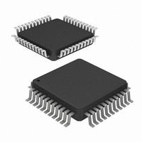
CONV A/D 16BIT 8:1 MUX 44-MQFP
Manufacturer
Intersil
Datasheet
1.HI7188IN.pdf
(24 pages)
Specifications of HI7188IN
Number Of Bits
16
Sampling Rate (per Second)
240
Data Interface
QSPI™, Serial, SPI™
Number Of Converters
1
Power Dissipation (max)
50mW
Voltage Supply Source
Analog and Digital, Dual ±
Operating Temperature
-40°C ~ 85°C
Mounting Type
Surface Mount
Package / Case
44-QFP
Lead Free Status / RoHS Status
Contains lead / RoHS non-compliant
Available stocks
Company
Part Number
Manufacturer
Quantity
Price


Pin Descriptions
5, 6, 27, 28
44 LEAD
4, 29, 39
MQFP
3, 30
41
42
43
44
10
11
12
13
14
15
16
17
18
19
20
21
22
23
24
25
26
31
32
33
34
35
36
37
38
40
1
2
7
8
9
PIN NAME
RSTI/O
MODE
DGND
OSC
OSC
DV
V
V
V
V
V
V
V
V
SCLK
AV
V
V
V
V
V
V
V
V
V
AV
SDIO
V
MXC
SDO
V
EOS
RST
INH1
INH2
INH3
INH4
INH5
INH6
INH7
INH8
CA
CS
INL1
INL2
INL3
INL4
INL5
INL6
INL7
INL8
RLO
A
A
A
RHI
CM
DD
SS
DD
0
1
2
1
2
5
Mode input. Used to select between Synchronous Self Clocking (MODE = 1) or Synchronous External Clocking
(MODE = 0) for the Serial Port.
Serial interface clock. Synchronizes serial data transfers. Data is input on the rising edge and output on the falling
edge.
Serial Data Out. Serial data is read from this line when using a 3-wire serial protocol such as the Motorola Serial
Peripheral Interface.
Serial Data IN or OUT. This line is bidirectional programmable and interfaces directly to the Intel Standard Serial
Interface using a 2-wire serial protocol.
Oscillator clock input for the device. A crystal connected between OSC
device, or an external oscillator can drive OSC
Noise Rejection.
Used to connect a crystal source between OSC
Positive Digital supply (+5V).
Digital supply ground.
Negative analog power supply (-5V).
Analog input low for Channel 1.
Analog input high for Channel 1.
Analog input low for Channel 2.
Analog input high for Channel 2.
Analog input low for Channel 3.
Analog input high for Channel 3.
Analog input low for Channel 4.
Analog input high for Channel 4.
Analog input low for Channel 5.
Analog input high for Channel 5.
Analog input low for Channel 6.
Analog input high for Channel 6.
Analog input low for Channel 7.
Analog input high for Channel 7.
Analog input low for Channel 8.
Analog input high for Channel 8.
Common mode voltage. Must be tied to the mid point of AV
External reference input. Should be negative referenced to V
External reference input. Should be positive referenced to V
Positive analog power supply (+5V).
Active low Reset pin. Used to initialize modulator, filter, RAMs, registers and state machines.
Calibration active output. Indicates that at least one active channel is in a calibration mode.
Multiplexer control output. Indicates that the conversion for the active channel is complete.
Logical channel count output (LSB).
Logical channel count output.
Logical channel count output (MSB).
End of scan output. Signals the end of a channel scan (all active channels have been converted) and data is
available to be read. Remains low until data RAM is read.
I/O reset (active low) input. Resets serial interface state machine only.
Active low chip select pin. Used to select a serial data transfer cycle. When high the SDO and SDIO pins are
three-state.
HI7188
PIN DESCRIPTION
1
. The oscillator frequency should be 3.6864MHz to maintain Line
1
and OSC
2
DD
. Leave open otherwise.
RLO
RHI
and AV
.
.
SS
1
.
and OSC
2
will provide a clock to the
Related parts for HI7188IN
Image
Part Number
Description
Manufacturer
Datasheet
Request
R

Part Number:
Description:
8-channel, 16-bit, High Precision, Sigma-delta A/d Sub-system
Manufacturer:
Intersil Corporation
Datasheet:
Part Number:
Description:
Intersil Corporation [CMOS Serial Controller Interface]
Manufacturer:
Intersil Corporation
Datasheet:
Part Number:
Description:
Manufacturer:
Intersil Corporation
Datasheet:
Part Number:
Description:
357-036-542-201 CARDEDGE 36POS DL .156 BLK LOPRO
Manufacturer:
Intersil Corporation
Datasheet:
Part Number:
Description:
1024-Word x 4-Bit LSI Static RAM
Manufacturer:
Intersil Corporation
Datasheet:
Part Number:
Description:
General Purpose NPN Transistor Arrays FN341.4
Manufacturer:
Intersil Corporation
Datasheet:
Part Number:
Description:
CMOS 16-Bit Microprocessor
Manufacturer:
Intersil Corporation
Datasheet:
Part Number:
Description:
Manufacturer:
Intersil Corporation
Datasheet:
Part Number:
Description:
Manufacturer:
Intersil Corporation
Datasheet:
Part Number:
Description:
Manufacturer:
Intersil Corporation
Datasheet:
Part Number:
Description:
Manufacturer:
Intersil Corporation
Datasheet:
Part Number:
Description:
CMOS 6-Bit Latch and Decoder Memory Interfaces
Manufacturer:
Intersil Corporation
Datasheet:
Part Number:
Description:
CA3046General Purpose NPN Transistor Arrays
Manufacturer:
Intersil Corporation
Datasheet:
Part Number:
Description:
Manufacturer:
Intersil Corporation
Datasheet:
Part Number:
Description:
TR909 DLC/FLC SLIC with Low Power Standby
Manufacturer:
Intersil Corporation
Datasheet: