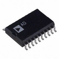
AD7302BRZ Analog Devices Inc, AD7302BRZ Datasheet - Page 10

AD7302BRZ
Manufacturer Part Number
AD7302BRZ
Description
IC DAC 8BIT DUAL R-R 20-SOIC
Manufacturer
Analog Devices Inc
Datasheet
1.AD7302BRUZ.pdf
(16 pages)
Specifications of AD7302BRZ
Data Interface
Parallel
Settling Time
1.2µs
Number Of Bits
8
Number Of Converters
2
Voltage Supply Source
Single Supply
Power Dissipation (max)
24.8mW
Operating Temperature
-40°C ~ 105°C
Mounting Type
Surface Mount
Package / Case
20-SOIC (7.5mm Width)
Resolution (bits)
8bit
Sampling Rate
833kSPS
Input Channel Type
Parallel
Supply Voltage Range - Analog
2.7V To 5.5V
Supply Current
2.8mA
Digital Ic Case Style
SOIC
Lead Free Status / RoHS Status
Lead free / RoHS Compliant
Available stocks
Company
Part Number
Manufacturer
Quantity
Price
Company:
Part Number:
AD7302BRZ
Manufacturer:
Maxim
Quantity:
25
Part Number:
AD7302BRZ
Manufacturer:
ADI/亚德诺
Quantity:
20 000
Part Number:
AD7302BRZ-REEL
Manufacturer:
ADI/亚德诺
Quantity:
20 000
AD7302
Automatic Update Mode
In this mode of operation the LDAC signal is permanently tied
low. The state of the LDAC is sampled on the rising edge of
WR. LDAC being low allows the selected DAC register to be
automatically updated on the rising edge of WR. The output
update occurs on the rising edge of WR. Figure 23 shows the
timing associated with the automatic update mode of operation
and also the status of the various registers during this frame.
Figure 23. Timing and Register Arrangement for Auto-
matic Update Mode
Simultaneous Update Mode
In this mode of operation the LDAC signal is used to update both
DAC outputs simultaneously. The state of the LDAC is sampled
on the rising edge of WR. If LDAC is high, the automatic update
mode is disabled and both DAC latches are updated at any time
after the write by taking LDAC low. The output update occurs
on the falling edge of LDAC. LDAC must be taken back high
again before the next data transfer takes place. Figure 24
shows the timing associated with the simultaneous update mode
of operation and also the status of the various registers during
this frame.
Figure 24. Timing and Register Arrangement for Simulta-
neous Update Mode
DAC REG (SLE)
DAC REG (SLE)
I/P REG (MLE)
I/P REG (MLE)
LDAC = 0
D7–D0
D7–D0
LDAC
V
V
OUT
OUT
A/B
A/B
WR
WR
CS
CS
TRACK
HOLD
HOLD
TRACK
TRACK
HOLD
HOLD
TRACK
HOLD
HOLD
TRACK
HOLD
–10–
POWER-ON RESET
The AD7302 has a power-on reset circuit designed to allow
output stability during power-up. This circuit holds the DACs
in a reset state until a write takes place to the DAC. In the reset
state all zeros are latched into the input registers of each DAC
and the DAC registers are in transparent mode, thus the output
of both DACs is held at ground potential until a write takes
place to the DAC. The power-on reset circuitry generates a
PON STRB signal, which is a gating signal used within the logic
to identify a power-on condition.
POWER-DOWN FEATURES
The AD7302 has a power-down feature. This is implemented
by exercising the external PD pin; an active low signal puts the
complete DAC into power-down mode. When in power-down
the current consumption of the device is reduced to 1 A max at
25 C and 2 A max over temperature, making the device
suitable for use in portable battery powered equipment. When
power-down is activated, the reference bias servo loop and the
output amplifiers with their associated linear circuitry are
powered down, the reference resistors are open circuited to
further reduce the power consumption. The output sees a load
of approximately 23 k to GND when in power-down mode as
shown in Figure 25. The contents of the data registers are
unaffected when in power-down mode. The device comes out
of power-down in typically 13 s (see Figure 10).
Analog Outputs
The AD7302 contains two independent voltage output DACs
with 8-bit resolution and rail-to-rail operation. The output buffer
provides a gain of two at the output. Figures 2 to 4 show the
source and sink capabilities of the output amplifier. The slew
rate of the output amplifier is typically 7.5 V/ s and has a full-
scale settling to 8 bits with a 100 pF capacitive load in typically
1.2 s.
The input coding to the DAC is straight binary. Table I shows
the binary transfer function for the AD7302. Figure 26 shows
the DAC transfer function for binary coding. Any DAC output
voltage can be expressed as:
where:
N
Figure 25. Output Stage During Power-Down
is the decimal equivalent of the binary input code.
N ranges from 0 to 255.
V
REF
I
V
DAC
OUT
= 2
11.7k
V
REF
(N/256)
V
11.7k
DD
REV. 0


