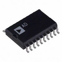
AD7302BRZ Analog Devices Inc, AD7302BRZ Datasheet - Page 12

AD7302BRZ
Manufacturer Part Number
AD7302BRZ
Description
IC DAC 8BIT DUAL R-R 20-SOIC
Manufacturer
Analog Devices Inc
Datasheet
1.AD7302BRUZ.pdf
(16 pages)
Specifications of AD7302BRZ
Data Interface
Parallel
Settling Time
1.2µs
Number Of Bits
8
Number Of Converters
2
Voltage Supply Source
Single Supply
Power Dissipation (max)
24.8mW
Operating Temperature
-40°C ~ 105°C
Mounting Type
Surface Mount
Package / Case
20-SOIC (7.5mm Width)
Resolution (bits)
8bit
Sampling Rate
833kSPS
Input Channel Type
Parallel
Supply Voltage Range - Analog
2.7V To 5.5V
Supply Current
2.8mA
Digital Ic Case Style
SOIC
Lead Free Status / RoHS Status
Lead free / RoHS Compliant
Available stocks
Company
Part Number
Manufacturer
Quantity
Price
Company:
Part Number:
AD7302BRZ
Manufacturer:
Maxim
Quantity:
25
Part Number:
AD7302BRZ
Manufacturer:
ADI/亚德诺
Quantity:
20 000
Part Number:
AD7302BRZ-REEL
Manufacturer:
ADI/亚德诺
Quantity:
20 000
AD7302
MICROPROCESSOR INTERFACING
AD7302–ADSP-2101/ADSP-2103 Interface
Figure 29 shows an interface between the AD7302 and the
ADSP-2101/ADSP-2103. The fast interface timing associated
with the AD7302 allows easy interface to the ADSP-2101/
ADSP-2103.
Two addresses are decoded to select loading data to either
DAC A or DAC B. LDAC is permanently tied low in this
circuit, so the selected DAC output is updated on the rising
edge of the WR signal.
Data is loaded to the AD7302 input register using the following
ADSP-21xx instruction:
MR0 = ADSP-21xx MR0 Register.
DAC = Decoded DAC Address.
AD7302–TMS32020 Interface
Figure 30 shows an interface between the AD7302 and the
TMS32020. The address decoder is used to decode the
addresses for DAC A and DAC B. Data is loaded to the
AD7302 using the following instruction:
DAC = Decoded DAC Address.
D = Data Memory Address.
Figure 29. AD7302–ADSP-2101/ADSP-2103 Interface
ADSP-2101*/
ADSP-2103*
DMA14
DMD15
DMA0
DMD0
DMS
WR
**ADDITIONAL CIRCUITRY OMITTED FOR CLARITY.
**A DECODED ADDRESS FOR DAC A.
**A+1 DECODED ADDRESS FOR DAC B.
EN
DM (DAC) = MR0
OUT DAC, D
DECODE
ADDR
ADDRESS BUS
A+1**
DATA BUS
A**
A/B
CS
LDAC
WR
DB7
DB0
AD7302*
–12–
In the circuit shown the LDAC is hardwired low, thus the
selected DAC output is updated on the rising edge of WR.
Some applications may require simultaneous updating of both
DACs in the AD7302. In this case the LDAC signal can be
driven from an external timer or can be controlled by the
microprocessor. One option for simultaneous updating is to
decode the LDAC from the address bus so that a write opera-
tion at this address will simultaneously update both DAC
outputs. A simple OR gate with one input driven from the
decoded address and the second input from the WR signal will
implement this function.
AD7302–8051/8088 Interface
Figure 31 shows a serial interface between the AD7302 and the
8051/8088 processors. The address decoder is used to decode
the addresses for DAC A and DAC B.
8051/8088
OR
TMS32020
ALE
AD7
AD0
A15
Figure 31. AD7302–8051//8088 Interface
Figure 30. AD7302–TMS32020 Interface
A8
DMD15
**ADDITIONAL CIRCUITRY OMITTED FOR CLARITY.
**A DECODED ADDRESS FOR DAC A.
**A+1 DECODED ADDRESS FOR DAC B.
DMD0
STRB
R/W
A15
A0
IS
OCTAL
LATCH
**ADDITIONAL CIRCUITRY OMITTED FOR CLARITY.
**A DECODED ADDRESS FOR DAC A.
**A+1 DECODED ADDRESS FOR DAC B.
EN
DECODE
ADDR
DECODE
ADDRESS/DATA BUS
ADDR
ADDRESS BUS
ADDRESS BUS
A+1**
DATA BUS
A**
A+1**
A**
A/B
CS
LDAC
WR
DB7
DB0
DB7
DB0
AD7302*
/B
AD7302*
REV. 0


