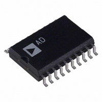
AD7302BRZ Analog Devices Inc, AD7302BRZ Datasheet - Page 9

AD7302BRZ
Manufacturer Part Number
AD7302BRZ
Description
IC DAC 8BIT DUAL R-R 20-SOIC
Manufacturer
Analog Devices Inc
Datasheet
1.AD7302BRUZ.pdf
(16 pages)
Specifications of AD7302BRZ
Data Interface
Parallel
Settling Time
1.2µs
Number Of Bits
8
Number Of Converters
2
Voltage Supply Source
Single Supply
Power Dissipation (max)
24.8mW
Operating Temperature
-40°C ~ 105°C
Mounting Type
Surface Mount
Package / Case
20-SOIC (7.5mm Width)
Resolution (bits)
8bit
Sampling Rate
833kSPS
Input Channel Type
Parallel
Supply Voltage Range - Analog
2.7V To 5.5V
Supply Current
2.8mA
Digital Ic Case Style
SOIC
Lead Free Status / RoHS Status
Lead free / RoHS Compliant
Available stocks
Company
Part Number
Manufacturer
Quantity
Price
Company:
Part Number:
AD7302BRZ
Manufacturer:
Maxim
Quantity:
25
Part Number:
AD7302BRZ
Manufacturer:
ADI/亚德诺
Quantity:
20 000
Part Number:
AD7302BRZ-REEL
Manufacturer:
ADI/亚德诺
Quantity:
20 000
GENERAL DESCRIPTION
D/A Section
The AD7302 is a dual 8-bit voltage output digital-to-analog
converter. The architecture consists of a reference amplifier, a
current source DAC followed by a current-to-voltage converter
capable of generating rail-to-rail voltages on the output of the
DAC. Figure 19 shows a block diagram of the basic DAC
architecture.
Both DAC A and DAC B outputs are internally buffered and
these output buffer amplifiers have rail-to-rail output character-
istics. The output amplifier is capable driving a load of 10 k to
both V
reference selection for the DAC can either be internally generated
from V
comparator on the REFIN pin detects whether the required
reference is the internally generated reference or the externally
applied voltage to the REFIN pin. If REFIN is connected to
V
reference. When an externally applied voltage is more than one
volt below V
externally applied voltage to the REFIN pin. The range on the
external reference input is from 1.0 V to V
voltage from either DAC is given by:
where:
Reference
The AD7302 has the facility to use either an external reference
applied through the REFIN pin or an internal reference
generated from V
arrangement where either the internal V
externally applied reference can be selected.
REV. 0
DD
REFIN
N
V
REF
, the reference selected is the internally generated V
EXT REF
INT REF
DD
DD
is the voltage applied to the external REFIN pin or
V
is the decimal equivalent of the code loaded to the DAC
register and ranges from 0 to 255.
V
DD
DD
or externally applied through the REFIN pin. A
and ground in parallel with a 100 pF to ground. The
Figure 20. Reference Selection Circuitry
30k
30k
/2 when the internal reference is selected.
DD
, the comparator selection switches to the
Figure 19. DAC Architecture
DD
REF
V
V
O
DD
. Figure 20 shows the reference input
IN
A/B = 2
REFERENCE
+
AMPLIFIER
-
REF
INT
PMOS
VTH
V
CURRENT
REF
DAC
COMPARATOR
11.7k
(N/256)
DD
MUX
DD
/2 reference or the
SELECTED
REFERENCE OUTPUT
/2. The output
AD7302
I/V
11.7k
DD
V
/2
O
A/B
–9–
The internal reference is selected by tying the REFIN pin to
V
applied to the REFIN pin; if this is 1 V below V
circuitry will select this externally applied reference as the
reference source for the DAC.
Digital Interface
The AD7302 contains a fast parallel interface allowing this dual
DAC to interface to industry standard microprocessors, micro-
controllers and DSP machines. There are two modes in which
this parallel interface can be configured to update the DAC
outputs. The simultaneous update mode allows simultaneous
updating of both DAC outputs. The automatic update mode
allows each DAC to be individually updated following a write
cycle. Figure 21 shows the internal logic associated with the
digital interface. The PON STRB signal is internally generated
from the power on reset circuitry and is low during the power-
on reset phase of the power-up procedure.
The AD7302 has a double buffered interface, which allows
for simultaneous updating of the DAC outputs. Figure 22 shows
a block diagram of the register arrangement within the AD7302.
DD
PON STRB
. If an external reference is to be used, this can be directly
LDAC
A/B
WR
CLR
CS
LDAC
CLR
A/B
WR
CS
Figure 22. Register Arrangement
Figure 21. Logic Interface
MLE
CONTROL
LOGIC
SLE
DECODER
REGISTER
DRIVERS
4 TO 15
LOWER
NIBBLE
DAC
4
15
15
30
REGISTER
DB7–DB0
DAC A SEL
ENABLE
ENABLE
CLEAR
SET SLE
CLEAR
SET SLE
DAC B SEL
LDAC
LDAC
INPUT
8
REGISTER
DECODER
DRIVERS
4 TO 15
NIBBLE
UPPER
AD7302
DD
DAC
CONTROL
CONTROL
DAC A
LOGIC
DAC B
LOGIC
, the internal
4
15
15
30
CLR
MLE A
SLE A
MLE B
SLE B


