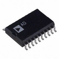
AD7302BRZ Analog Devices Inc, AD7302BRZ Datasheet - Page 14

AD7302BRZ
Manufacturer Part Number
AD7302BRZ
Description
IC DAC 8BIT DUAL R-R 20-SOIC
Manufacturer
Analog Devices Inc
Datasheet
1.AD7302BRUZ.pdf
(16 pages)
Specifications of AD7302BRZ
Data Interface
Parallel
Settling Time
1.2µs
Number Of Bits
8
Number Of Converters
2
Voltage Supply Source
Single Supply
Power Dissipation (max)
24.8mW
Operating Temperature
-40°C ~ 105°C
Mounting Type
Surface Mount
Package / Case
20-SOIC (7.5mm Width)
Resolution (bits)
8bit
Sampling Rate
833kSPS
Input Channel Type
Parallel
Supply Voltage Range - Analog
2.7V To 5.5V
Supply Current
2.8mA
Digital Ic Case Style
SOIC
Lead Free Status / RoHS Status
Lead free / RoHS Compliant
Available stocks
Company
Part Number
Manufacturer
Quantity
Price
Company:
Part Number:
AD7302BRZ
Manufacturer:
Maxim
Quantity:
25
Part Number:
AD7302BRZ
Manufacturer:
ADI/亚德诺
Quantity:
20 000
Part Number:
AD7302BRZ-REEL
Manufacturer:
ADI/亚德诺
Quantity:
20 000
AD7302
Programmable Current Source
Figure 35 shows the AD7302 used as the control element of a
programmable current source. In this circuit the full-scale
current is set to 1 mA. The output voltage from the DAC is
applied across the current setting resistor of 4.7 k in series
with the full-scale setting resistor of 470 . Transistors suitable
to place in the feedback loop of the amplifier include the BC107
or the 2N3904, which enable the current source to operate from
a min V
the operating characteristics of the of the transistor. Suitable
amplifiers include the AD820 and the OP295 both having rail-
to-rail operation on their outputs. The current for any digital
input code can be calculated as follows:
Coarse and Fine Adjustment Using the AD7302
The DACs on the AD7302 can be paired together to form a
coarse and fine adjustment function as shown in Figure 36. In
this circuit DAC A is used to provide the coarse function while
DAC B is used to provide the fine adjustment. Varying the ratio
of R1 and R2 will vary the relative effect of the coarse and fine
tune elements in the circuit. For the resistor values shown
DAC B has a resolution of 148 V giving a fine tune range of
approximately 2 LSBs for operation with a V
reference of 2.5 V. The amplifiers shown allow a rail-to-rail
output voltage to be achieved on the output. A typical applica-
tion for such a circuit would be in a setpoint controller.
EXT REF
AD780/REF192
WITH V
GND
V
SOURCE
IN
DD
Figure 35. Programmable Current Source
V
= 5V
OUT
I = 2 V
of 6 V. The operating range is determined by
0.1µF
REF
0.1µF
REF IN
AD7302
D/(5E +3 256) mA
10µF
V
AGND
DD
V
DD
= 5V
V
DGND
OUT
A
DD
AD820/
OP295
of 5 V and a
+5V
V
SOURCE
LOAD
4.7k
470
–14–
Power Supply Bypassing and Grounding
In any circuit where accuracy is important, careful consideration
of the power supply and ground return layout helps to ensure
the rated performance. The printed circuit board on which the
AD7302 is mounted should be designed so the analog and
digital sections are separated and confined to certain areas of the
board. If the AD7302 is in a system where multiple devices
require an AGND to DGND connection, the connection should
be made at one point only, a star ground point that should be
established as closely as possible to the AD7302. The AD7302
should have ample supply bypassing of 10 F in parallel with
0.1 F on the supply located as close to the package as possible,
ideally right up against the device. The 10 F capacitors are the
tantalum bead type. The 0.1 F capacitor should have low
Effective Series Resistance (ESR) and Effective Series Induc-
tance (ESI), such as the common ceramic types, which provide
a low impedance path to ground at high frequencies to handle
transient currents due to internal logic switching.
The power supply lines of the AD7302 should use as large a
trace as possible to provide low impedance paths and reduce the
effects of glitches on the power supply line. Fast switching sig-
nals like clocks should be shielded with digital ground to avoid
radiating noise to other parts of the board and should never be
run near the reference inputs. Avoid crossover of digital and
analog signals. Traces on opposite sides of the board should run
at right angles to each other. This reduces the effects of feed-
through through the board. A microstrip technique is by far the
best, but not always possible with a double-sided board. In this
technique, the component side of the board is dedicated to
ground plane while signal traces are placed on the solder side.
AD589 WITH V
EXT REF
AD780/REF192
WITH V
GND
V
OR
IN
DD
V
= 5V
DD
OUT
Figure 36. Coarse/Fine Adjust Circuit
= 3V
0.1µF
0.1µF
REF IN
AD7302
10µF
AGND
V
DD
V
DD
= 5V
DGND
V
V
OUT
OUT
51.2k
R3
A
B
51.2k
390
R1
R2
AD820/
OP295
390
R4
+5V
REV. 0
V
OUT


