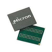
MT46H16M32LFCM-75 L Micron Technology Inc, MT46H16M32LFCM-75 L Datasheet - Page 71

MT46H16M32LFCM-75 L
Manufacturer Part Number
MT46H16M32LFCM-75 L
Description
Manufacturer
Micron Technology Inc
Type
DDR SDRAMr
Datasheet
1.MT46H16M32LFCM-75_L.pdf
(98 pages)
Specifications of MT46H16M32LFCM-75 L
Organization
16Mx32
Density
512Mb
Address Bus
15b
Access Time (max)
6.5/6ns
Maximum Clock Rate
133MHz
Operating Supply Voltage (typ)
1.8V
Package Type
VFBGA
Operating Temp Range
0C to 70C
Operating Supply Voltage (max)
1.95V
Operating Supply Voltage (min)
1.7V
Supply Current
100mA
Pin Count
90
Mounting
Surface Mount
Operating Temperature Classification
Commercial
Lead Free Status / Rohs Status
Compliant
WRITE Operation
PDF: 09005aef82d5d305
512mb_ddr_mobile_sdram_t47m.pdf – Rev. I 12/09 EN
WRITE bursts are initiated with a WRITE command, as shown in Figure 12 (page 39).
The starting column and bank addresses are provided with the WRITE command, and
auto precharge is either enabled or disabled for that access. If auto precharge is ena-
bled, the row being accessed is precharged at the completion of the burst. For the
WRITE commands used in the following illustrations, auto precharge is disabled. Basic
data input timing is shown in Figure 33 (page 72) (this timing applies to all WRITE
operations).
Input data appearing on the data bus is written to the memory array subject to the state
of data mask (DM) inputs coincident with the data. If DM is registered LOW, the corre-
sponding data will be written; if DM is registered HIGH, the corresponding data will be
ignored, and the write will not be executed to that byte/column location. DM operation
is illustrated in Figure 34 (page 73).
During WRITE bursts, the first valid data-in element will be registered on the first rising
edge of DQS following the WRITE command, and subsequent data elements will be reg-
istered on successive edges of DQS. The LOW state of DQS between the WRITE com-
mand and the first rising edge is known as the write preamble; the LOW state of DQS
following the last data-in element is known as the write postamble. The WRITE burst is
complete when the write postamble and
The time between the WRITE command and the first corresponding rising edge of DQS
(
WRITE diagrams show the nominal case. Where the two extreme cases (that is,
[MIN] and
(page 74) shows the nominal case and the extremes of
completion of a burst, assuming no other commands have been initiated, the DQ will
remain High-Z and any additional input data will be ignored.
Data for any WRITE burst can be concatenated with or truncated by a subsequent
WRITE command. In either case, a continuous flow of input data can be maintained.
The new WRITE command can be issued on any positive edge of clock following the
previous WRITE command. The first data element from the new burst is applied after
either the last element of a completed burst or the last desired data element of a longer
burst that is being truncated. The new WRITE command should be issued x cycles after
the first WRITE command, where x equals the number of desired data element pairs
(pairs are required by the 2n-prefetch architecture).
Figure 36 (page 75) shows concatenated bursts of 4. An example of nonconsecutive
WRITEs is shown in Figure 37 (page 75). Full-speed random write accesses within a
page or pages can be performed, as shown in Figure 38 (page 76).
Data for any WRITE burst can be followed by a subsequent READ command. To follow
a WRITE without truncating the WRITE burst,
ure 39 (page 77).
Data for any WRITE burst can be truncated by a subsequent READ command, as shown
in Figure 40 (page 78). Note that only the data-in pairs that are registered prior to the
t
masked with DM, as shown in Figure 41 (page 79).
Data for any WRITE burst can be followed by a subsequent PRECHARGE command. To
follow a WRITE without truncating the WRITE burst,
Figure 42 (page 80).
WTR period are written to the internal array, and any subsequent data-in should be
t
DQSS) is specified with a relatively wide range (75%–125% of one clock cycle). All
t
DQSS [MAX]) might not be obvious, they have also been included. Figure 35
71
512Mb: x16, x32 Mobile LPDDR SDRAM
Micron Technology, Inc. reserves the right to change products or specifications without notice.
t
WR or
t
WTR should be met, as shown in Fig-
t
WTR are satisfied.
t
WR should be met, as shown in
t
DQSS for a burst of 4. Upon
© 2004 Micron Technology, Inc. All rights reserved.
WRITE Operation
t
DQSS


