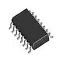
SI3018-F-FSR Silicon Laboratories Inc, SI3018-F-FSR Datasheet - Page 13

SI3018-F-FSR
Manufacturer Part Number
SI3018-F-FSR
Description
Modem Chip Chipset 16-Pin SOIC T/R
Manufacturer
Silicon Laboratories Inc
Datasheet
1.SI3018-F-FSR.pdf
(112 pages)
Specifications of SI3018-F-FSR
Package
16SOIC
Main Category
Chipset
Sub-category
Data/Voice
Typical Operating Supply Voltage
3.3 V
Power Supply Type
Digital
Typical Supply Current
8.5 mA
Minimum Operating Supply Voltage
3 V
Maximum Operating Supply Voltage
3.6 V
Data Rate
54.6875Kbps
Operating Supply Voltage (typ)
3.3V
Operating Supply Voltage (min)
3V
Operating Supply Voltage (max)
3.6V
Operating Temp Range
0C to 70C
Operating Temperature Classification
Commercial
Pin Count
16
Mounting
Surface Mount
Lead Free Status / Rohs Status
Compliant
Available stocks
Company
Part Number
Manufacturer
Quantity
Price
Company:
Part Number:
SI3018-F-FSR
Manufacturer:
SiliconL
Quantity:
52 026
Company:
Part Number:
SI3018-F-FSR
Manufacturer:
SILICON
Quantity:
57
Part Number:
SI3018-F-FSR
Manufacturer:
SILICONLABS/芯科
Quantity:
20 000
Table 9. Switching Characteristics—GCI Highway Serial Interface
(V
Parameter
Cycle Time PCLK (Single Clocking Mode)
Cycle Time PCLK (Double Clocking Mode)
Valid PCLK Inputs
FSYNC Period
PCLK Duty Cycle
PCLK Jitter Tolerance
FSYNC Jitter Tolerance
Rise Time, PCLK
Fall Time, PCLK
Delay Time, PCLK Rise to DTX Active
Delay Time, PCLK Rise to DTX Transition
Delay Time, PCLK Rise to DTX Tri-State
Setup Time, FSYNC Rise to PCLK Fall
Hold Time, PCLK Fall to FSYNC Fall
Setup Time, DRX Transition to PCLK Fall
Hold Time, PCLK Falling to DRX Transition
Notes:
D
=
1. All timing is referenced to the 50% level of the waveform. Input test levels are V
2. FSYNC must be 8 kHz under all operating conditions.
3. Specification applies to PCLK fall to DTX tri-state when that mode is selected.
3.0 to 3.6 V, T
times are referenced to the 20% and 80% levels of the waveform.
1
2
FSYNC
DRX
PCLK
DTX
A
Figure 5. GCI Highway Interface Timing Diagram (1x PCLK Mode)
=
0 to 70 °C for K-Grade, C
t
d1
t
su1
t
h1
3
L
=
Symbol
20 pF)
t
t
t
t
t
jitter
jitter
t
t
t
t
t
su1
su2
t
t
t
dty
d1
d2
d3
h1
h2
t
t
fp
p
p
r
f
t
Rev. 1.31
su2
t
d2
t
p
Conditions
t
h2
t
fp
Test
t
Si3050 + Si3018/19
r
Min
40
25
20
25
20
—
—
—
—
—
—
—
—
—
—
—
—
IH
=
V
O
– 0.4 V, V
2.048
4.096
Typ
488
244
125
50
t
—
—
—
—
—
—
—
—
—
—
—
f
t
d3
IL
=
0.4 V, rise and fall
±120
Max
60
25
25
20
20
20
—
—
—
—
—
—
—
—
—
2
Units
MHz
MHz
ns
ns
µs
ns
ns
ns
ns
ns
ns
ns
ns
ns
ns
ns
%
13


