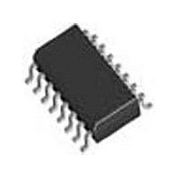
SI3018-F-FSR Silicon Laboratories Inc, SI3018-F-FSR Datasheet - Page 82

SI3018-F-FSR
Manufacturer Part Number
SI3018-F-FSR
Description
Modem Chip Chipset 16-Pin SOIC T/R
Manufacturer
Silicon Laboratories Inc
Datasheet
1.SI3018-F-FSR.pdf
(112 pages)
Specifications of SI3018-F-FSR
Package
16SOIC
Main Category
Chipset
Sub-category
Data/Voice
Typical Operating Supply Voltage
3.3 V
Power Supply Type
Digital
Typical Supply Current
8.5 mA
Minimum Operating Supply Voltage
3 V
Maximum Operating Supply Voltage
3.6 V
Data Rate
54.6875Kbps
Operating Supply Voltage (typ)
3.3V
Operating Supply Voltage (min)
3V
Operating Supply Voltage (max)
3.6V
Operating Temp Range
0C to 70C
Operating Temperature Classification
Commercial
Pin Count
16
Mounting
Surface Mount
Lead Free Status / Rohs Status
Compliant
Available stocks
Company
Part Number
Manufacturer
Quantity
Price
Company:
Part Number:
SI3018-F-FSR
Manufacturer:
SiliconL
Quantity:
52 026
Company:
Part Number:
SI3018-F-FSR
Manufacturer:
SILICON
Quantity:
57
Part Number:
SI3018-F-FSR
Manufacturer:
SILICONLABS/芯科
Quantity:
20 000
Si3050 + Si3018/19
Register 31. DAA Control 5
Reset settings = 0010_0000
82
6:5
Bit
7
4
3
2
1
0
Name
Type
Bit
Reserved Always write these bits to zero.
Reserved Always write these bits to zero.
FOH[1:0] Fast Off-Hook Selection.
Name
OHS2
FULL
LVFD
FILT
FULL
R/W
Full Scale Transmit and Receive Mode.
0 = Default.
1 = Transmit/receive full scale.
This bit changes the full scale of the ADC and DAC from 0 dBm min to +3.2 dBm into a 600
load (or 1 dBV into all reference impedances). When this bit is set, the DCV[1:0] bits
(Register 26) should be set to all 1s. The MINI[1:0] bits also should be set to all 0s. This ensures
correct operation of the full scale mode.
These bits determine the length of the off-hook counter. The default setting is 128 ms.
00 = 512 ms
01 = 128 ms
10 = 64 ms
11 = 8 ms
On-Hook Speed 2.
Filter Pole Selection.
0 = The receive path has a low –3 dBFS corner at 5 Hz.
1 = The receive path has a low –3 dBFS corner at 200 Hz.
Line Voltage Force Disable (Si3019 line-side only).
0 = Normal operation.
1 = The circuitry that forces the LVS register (Register 29) to all 0s at 3 V or less is disabled. The
LVS register may display unpredictable values at voltages between 0 to 2 V. All 0s are displayed
if the line voltage is 0 V.
This bit, in combination with the OHS bit (Register 16) and the SQ[1:0] bits on-hook speeds
specified are measured from the time the OH bit is cleared until loop current equals zero.
OHS
D7
0
0
1
OHS2
D6
0
1
X
FOH[1:0]
RW
SQ[1:0]
D5
00
00
11
Rev. 1.31
D4
0
26 ms ±10% (meets Australia spark quenching spec)
Mean On-Hook Speed
Less than 0.5 ms
3 ms ±10% (meets ETSI standard)
Function
OHS2
R/W
D3
D2
0
FILT
R/W
D1
LVFD
R/W
D0


