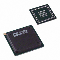
ADSP-BF532SBB400 Analog Devices Inc, ADSP-BF532SBB400 Datasheet - Page 18

ADSP-BF532SBB400
Manufacturer Part Number
ADSP-BF532SBB400
Description
IC DSP CTLR 16BIT 400MHZ 169-BGA
Manufacturer
Analog Devices Inc
Series
Blackfin®r
Type
Fixed Pointr
Datasheet
1.ADSP-BF531SBSTZ400.pdf
(12 pages)
Specifications of ADSP-BF532SBB400
Interface
SPI, SSP, UART
Clock Rate
400MHz
Non-volatile Memory
ROM (1 kB)
On-chip Ram
84kB
Voltage - I/o
1.8V, 2.5V, 3.3V
Voltage - Core
1.20V
Operating Temperature
-40°C ~ 85°C
Mounting Type
Surface Mount
Package / Case
169-BGA
For Use With
ADZS-BF533-EZLITE - KIT W/BOARD EVAL FOR ADSP-BF533
Lead Free Status / RoHS Status
Lead free / RoHS Compliant
ADSP-BF531/BF532/BF533
32.
33.
34.
DESCRIPTION:
In this mode, if the PORT_CFG field in the PPI_CONTROL register is set to #b11 (Sync PPI_FS3 to PPI_FS2), the PPI_FS3 frame sync signal is
not driven to the PF3 flag pin. It is, however, correctly driven to PF3 when the PORT_CFG field is set to #b01 (Sync PPI_FS3 to PPI_FS1).
WORKAROUND:
None
APPLIES TO REVISION(S):
0.3, 0.4, 0.5
DESCRIPTION:
The DSPID register does not contain the correct silicon revision information.
WORKAROUND:
The upper 4 bits of the REVID register (at address 0xFFC0 0014) can be read to obtain silicon revision information. The remaining bits at
this location are reserved.
APPLIES TO REVISION(S):
0.4
DESCRIPTION:
If the DF bit is set prior to a hardware reset, the PLL will continue to divide CLKIN by 2 after the hardware reset, but the DF bit itself will be
cleared in the PLL_CTL register.
WORKAROUND:
Reprogram the PLL with DF cleared if the desire is to not divide CLKIN by 2 after reset.
APPLIES TO REVISION(S):
0.3, 0.4
05000233 - PPI_FS3 Is Not Driven in 2 or 3 Internal Frame Sync Transmit Modes:
05000234 - Incorrect Revision Number in DSPID Register:
05000242 - DF Bit in PLL_CTL Register Does Not Respond to Hardware Reset:
NR003532D | Page 18 of 45 | July 2008
Silicon Anomaly List


