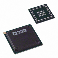
ADSP-BF532SBB400 Analog Devices Inc, ADSP-BF532SBB400 Datasheet - Page 29

ADSP-BF532SBB400
Manufacturer Part Number
ADSP-BF532SBB400
Description
IC DSP CTLR 16BIT 400MHZ 169-BGA
Manufacturer
Analog Devices Inc
Series
Blackfin®r
Type
Fixed Pointr
Datasheet
1.ADSP-BF531SBSTZ400.pdf
(12 pages)
Specifications of ADSP-BF532SBB400
Interface
SPI, SSP, UART
Clock Rate
400MHz
Non-volatile Memory
ROM (1 kB)
On-chip Ram
84kB
Voltage - I/o
1.8V, 2.5V, 3.3V
Voltage - Core
1.20V
Operating Temperature
-40°C ~ 85°C
Mounting Type
Surface Mount
Package / Case
169-BGA
For Use With
ADZS-BF533-EZLITE - KIT W/BOARD EVAL FOR ADSP-BF533
Lead Free Status / RoHS Status
Lead free / RoHS Compliant
Silicon Anomaly List
50.
DESCRIPTION:
The internal voltage regulator is susceptible to supply and ground noise transients induced by high I/O activity, particularly in cases of
high VDDext. This can result in a higher VDDint than the value that was programmed. In some cases, the value increases to a number
outside the upper spec of the range in the data sheet. VDDint returns to the programmed value when the I/O activity diminishes or stops.
To date, increased voltages that have exceeded the upper end of the spec value have only been observed while running tests with
artificially high I/O activity (e.g., when all bits of the address and data lines toggle every clock). Out-of-spec behavior has not been
observed in any customer application running application code.
WORKAROUND:
This problem does not occur if an external voltage regulator is used. To determine if the problem exists in your application, you should
monitor the VDDint waveform under the following conditions/setup:
• Apply the maximum VDDext based on the tolerance of VDDext supply.
• Run the application in a steady state (non-startup) condition.
• Connect an oscilloscope with minimum ground and signal loops to VDDint.
• Set the oscilloscope to trigger on a VDDint value that is between a number that is 10% higher than your programmed value and the
absolute maximum voltage (see data-sheet for maximum Vddint specification), in order to avoid normal transients.
Not all parts are equally susceptible to this issue. Repeat the above monitoring on a minimum of 10 devices.
If the issue does occur, the value of VDDint will increase during periods of high I/O activity. If the max value of VDDint remains at or below
the maximum VDDint, there will be no long term reliability issues, but power consumption will be higher.
Since the problem is a function of VDDext, I/O activity, and the programmed value of VDDint, the following techniques may
mitigate/improve this issue:
• The problem is more likely to occur with VDDext values above 3.3V, so it is best to use a 3.3V (or less) regulator with a tolerance of +/- 2%
or better.
• Ensure adequate bypassing on VDDext.
• Reduce the I/O activity if possible (for example, operate at a lower SCLK frequency rate).
• Follow the requirements in application note EE-228. In addition, use a PMOS FET with the lowest gate charge ratings consistent with
your application's current rating needs.
APPLIES TO REVISION(S):
0.3, 0.4
Devices in BGA packages are more susceptible than devices in LQFP packages.
05000269 - High I/O Activity Causes Output Voltage of Internal Voltage Regulator (Vddint) to Increase:
NR003532D | Page 29 of 45 | July 2008
ADSP-BF531/BF532/BF533


