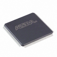
EP1C6T144C8 Altera, EP1C6T144C8 Datasheet - Page 52

EP1C6T144C8
Manufacturer Part Number
EP1C6T144C8
Description
IC CYCLONE FPGA 5980 LE 144-TQFP
Manufacturer
Altera
Series
Cyclone®r
Datasheet
1.EP1C3T144C8.pdf
(106 pages)
Specifications of EP1C6T144C8
Number Of Logic Elements/cells
5980
Number Of Labs/clbs
598
Total Ram Bits
92160
Number Of I /o
98
Voltage - Supply
1.425 V ~ 1.575 V
Mounting Type
Surface Mount
Operating Temperature
0°C ~ 85°C
Package / Case
144-TQFP, 144-VQFP
Family Name
Cyclone®
Number Of Logic Blocks/elements
5980
# I/os (max)
98
Frequency (max)
275.03MHz
Process Technology
0.13um (CMOS)
Operating Supply Voltage (typ)
1.5V
Logic Cells
5980
Ram Bits
92160
Operating Supply Voltage (min)
1.425V
Operating Supply Voltage (max)
1.575V
Operating Temp Range
0C to 85C
Operating Temperature Classification
Commercial
Mounting
Surface Mount
Pin Count
144
Package Type
TQFP
Lead Free Status / RoHS Status
Contains lead / RoHS non-compliant
Number Of Gates
-
Lead Free Status / Rohs Status
Not Compliant
Other names
544-1058
Available stocks
Company
Part Number
Manufacturer
Quantity
Price
Company:
Part Number:
EP1C6T144C8
Manufacturer:
ALTERA
Quantity:
7
Company:
Part Number:
EP1C6T144C8
Manufacturer:
ALTERA
Quantity:
85
Company:
Part Number:
EP1C6T144C8N
Manufacturer:
RAIO
Quantity:
5 600
Company:
Part Number:
EP1C6T144C8N
Manufacturer:
ALTERA
Quantity:
586
Part Number:
EP1C6T144C8N
Manufacturer:
ALTERA/阿尔特拉
Quantity:
20 000
Part Number:
EP1C6T144C8NNY
Manufacturer:
ALTERA
Quantity:
20 000
Cyclone Device Handbook, Volume 1
2–46
Preliminary
to automatically minimize setup time while providing a zero hold time.
Programmable delays can increase the register-to-pin delays for output
registers.
There are two paths in the IOE for a combinatorial input to reach the logic
array. Each of the two paths can have a different delay. This allows you
adjust delays from the pin to internal LE registers that reside in two
different areas of the device. The designer sets the two combinatorial
input delays by selecting different delays for two different paths under
the Decrease input delay to internal cells logic option in the Quartus II
software. When the input signal requires two different delays for the
combinatorial input, the input register in the IOE is no longer available.
The IOE registers in Cyclone devices share the same source for clear or
preset. The designer can program preset or clear for each individual IOE.
The designer can also program the registers to power up high or low after
configuration is complete. If programmed to power up low, an
asynchronous clear can control the registers. If programmed to power up
high, an asynchronous preset can control the registers. This feature
prevents the inadvertent activation of another device's active-low input
upon power up. If one register in an IOE uses a preset or clear signal then
all registers in the IOE must use that same signal if they require preset or
clear. Additionally a synchronous reset signal is available to the designer
for the IOE registers.
External RAM Interfacing
Cyclone devices support DDR SDRAM and FCRAM interfaces at up to
133 MHz through dedicated circuitry.
DDR SDRAM and FCRAM
Cyclone devices have dedicated circuitry for interfacing with DDR
SDRAM. All I/O banks support DDR SDRAM and FCRAM I/O pins.
However, the configuration input pins in bank 1 must operate at 2.5 V
because the SSTL-2 V
Input pin to logic array delay
Input pin to input register delay
Output pin delay
Table 2–9. Cyclone Programmable Delay Chain
Programmable Delays
Table 2–9
shows the programmable delays for Cyclone devices.
CCIO
level is 2.5 V. Additionally, the configuration
Decrease input delay to internal cells
Decrease input delay to input registers
Increase delay to output pin
Quartus II Logic Option
Altera Corporation
May 2008


