EP2C35F672C8 Altera, EP2C35F672C8 Datasheet - Page 62
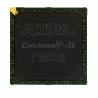
EP2C35F672C8
Manufacturer Part Number
EP2C35F672C8
Description
IC CYCLONE II FPGA 33K 672-FBGA
Manufacturer
Altera
Series
Cyclone® IIr
Datasheet
1.EP2C5T144C8N.pdf
(168 pages)
Specifications of EP2C35F672C8
Number Of Logic Elements/cells
33216
Number Of Labs/clbs
2076
Total Ram Bits
483840
Number Of I /o
475
Voltage - Supply
1.15 V ~ 1.25 V
Mounting Type
Surface Mount
Operating Temperature
0°C ~ 85°C
Package / Case
672-FBGA
Family Name
Cyclone® II
Number Of Logic Blocks/elements
33216
# I/os (max)
475
Frequency (max)
402.58MHz
Process Technology
90nm
Operating Supply Voltage (typ)
1.2V
Logic Cells
33216
Ram Bits
483840
Operating Supply Voltage (min)
1.15V
Operating Supply Voltage (max)
1.25V
Operating Temp Range
0C to 85C
Operating Temperature Classification
Commercial
Mounting
Surface Mount
Pin Count
672
Package Type
FBGA
For Use With
NANO-CYCLONE - KIT NANOBOARD AND CYCLONEII DC807-1002 - DAUGHTER CARD ALTERA CYCLONE IIP0301 - DE2 CALL FOR ACADEMIC PRICING544-1733 - PCI KIT W/CYCLONE II EP2C35N
Lead Free Status / RoHS Status
Contains lead / RoHS non-compliant
Number Of Gates
-
Lead Free Status / Rohs Status
Not Compliant
Other names
544-1089
EP2C35F672C8ES
EP2C35F672C8ES
Available stocks
Company
Part Number
Manufacturer
Quantity
Price

Part Number:
EP2C35F672C8
Manufacturer:
ALTERA
Quantity:
20 000
Company:
Part Number:
EP2C35F672C8N
Manufacturer:
YAGEO
Quantity:
500 000
Company:
Part Number:
EP2C35F672C8N
Manufacturer:
ALTERA
Quantity:
500
Part Number:
EP2C35F672C8N
Manufacturer:
ALTERA/阿尔特拉
Quantity:
20 000


I/O Structure & Features
2–50
Cyclone II Device Handbook, Volume 1
Open-Drain Output
Cyclone II devices provide an optional open-drain (equivalent to an
open-collector) output for each I/O pin. This open-drain output enables
the device to provide system-level control signals (that is, interrupt and
write-enable signals) that can be asserted by any of several devices.
Note to
(1)
LVCMOS (1.5 V)
SSTL-2 class I
SSTL-2 class II
SSTL-18 class I
SSTL-18 class II
HSTL-18 class I
HSTL-18 class II
HSTL-15 class I
HSTL-15 class II
Table 2–16. Programmable Drive Strength (Part 2 of 2)
The default current in the Quartus II software is the maximum setting for each
I/O standard.
I/O Standard
Table
2–16:
Top & Bottom I/O Pins
I
OH
/I
12
16
20
24
10
12
16
18
10
12
16
18
20
10
12
16
OL
2
4
6
8
8
6
8
8
8
Current Strength Setting (mA)
Altera Corporation
Side I/O Pins
Note (1)
February 2007
12
16
10
10
12
2
4
6
8
6
8
8
8
Related parts for EP2C35F672C8
Image
Part Number
Description
Manufacturer
Datasheet
Request
R

Part Number:
Description:
CYCLONE II STARTER KIT EP2C20N
Manufacturer:
Altera
Datasheet:


Part Number:
Description:
CPLD, EP610 Family, ECMOS Process, 300 Gates, 16 Macro Cells, 16 Reg., 16 User I/Os, 5V Supply, 35 Speed Grade, 24DIP
Manufacturer:
Altera Corporation
Datasheet:
Part Number:
Description:
CPLD, EP610 Family, ECMOS Process, 300 Gates, 16 Macro Cells, 16 Reg., 16 User I/Os, 5V Supply, 15 Speed Grade, 24DIP
Manufacturer:
Altera Corporation
Datasheet:
Part Number:
Description:
Manufacturer:
Altera Corporation
Datasheet:
Part Number:
Description:
CPLD, EP610 Family, ECMOS Process, 300 Gates, 16 Macro Cells, 16 Reg., 16 User I/Os, 5V Supply, 30 Speed Grade, 24DIP
Manufacturer:
Altera Corporation
Datasheet:
Part Number:
Description:
High-performance, low-power erasable programmable logic devices with 8 macrocells, 10ns
Manufacturer:
Altera Corporation
Datasheet:
Part Number:
Description:
High-performance, low-power erasable programmable logic devices with 8 macrocells, 7ns
Manufacturer:
Altera Corporation
Datasheet:
Part Number:
Description:
Classic EPLD
Manufacturer:
Altera Corporation
Datasheet:
Part Number:
Description:
High-performance, low-power erasable programmable logic devices with 8 macrocells, 10ns
Manufacturer:
Altera Corporation
Datasheet:
Part Number:
Description:
Manufacturer:
Altera Corporation
Datasheet:
Part Number:
Description:
Manufacturer:
Altera Corporation
Datasheet:
Part Number:
Description:
Manufacturer:
Altera Corporation
Datasheet:
Part Number:
Description:
CPLD, EP610 Family, ECMOS Process, 300 Gates, 16 Macro Cells, 16 Reg., 16 User I/Os, 5V Supply, 25 Speed Grade, 24DIP
Manufacturer:
Altera Corporation
Datasheet: