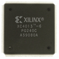
XC4013-6PQ240C Xilinx Inc, XC4013-6PQ240C Datasheet - Page 21

XC4013-6PQ240C
Manufacturer Part Number
XC4013-6PQ240C
Description
IC LOGIC CL ARRAY 13K GAT 240PQ
Manufacturer
Xilinx Inc
Series
XC4000r
Datasheet
1.XC4003-6PQ100C.pdf
(40 pages)
Specifications of XC4013-6PQ240C
Number Of Logic Elements/cells
1368
Number Of Labs/clbs
576
Total Ram Bits
18432
Number Of I /o
192
Number Of Gates
13000
Voltage - Supply
4.75 V ~ 5.25 V
Mounting Type
Surface Mount
Operating Temperature
0°C ~ 85°C
Package / Case
240-BFQFP
Lead Free Status / RoHS Status
Contains lead / RoHS non-compliant
Other names
122-1074
Available stocks
Company
Part Number
Manufacturer
Quantity
Price
SAMPLE PRELOAD
(* if PROGRAM = High)
Figure 20. Start-up Sequence
SAMPLE/PRELOAD
SAMPLE/PRELOAD
Boundary Scan
CONFIGURE
CONFIGURE*
READBACK
Instructions
Available:
EXTEST*
BYPASS
BYPASS
BYPASS
EXTEST
USER 1
USER 2
Master CCLK
Goes Active
If Boundary Scan
is Selected
F
Configuration Memory
Configuration Memory
One Time-Out Pulse
Test M0 Generate
Completely Clear
Data to DOUT
of 16 or 64 ms
Keep Clearing
Configuration
Configuration
Count Equals
Data Frame
Operational
Mode Lines
Once More
Yes
Yes
Yes
Sequence
Load One
No
Start-Up
memory
High? if
Sample
Config-
Master
Frame
uration
Length
>3.5 V
CCLK
Count
Error
Pass
V
INIT
Full
CC
Yes
Yes
No
No
No
No
Master Waits 50 to 250 s
Before Sampling Mode Lines
~1.3 s per Frame
Pull INIT Low
and Stop
PROGRAM
= Low
Yes
X6076
2-27
device when it recognizes the 0010 preamble. Following
the length-count data, any LCA device outputs a High on
DOUT until it has received its required number of data
frames.
After an LCA device has received its configuration data, it
passes on any additional frame start bits and configuration
data on DOUT. When the total number of configuration
clocks applied after memory initialization equals the value
of the 24-bit length count, the LCA device(s) begin the
start-up sequence and become operational together.
Configuration Sequence
Configuration Memory Clear
When power is first applied or reapplied to an LCA device,
an internal circuit forces initialization of the configuration
logic. When V
circuit passes the write and read test of a sample pair of
configuration bits, a nominal 16-ms time delay is started
(four times longer when M0 is Low, i.e., in Master mode).
During this time delay, or as long as the PROGRAM input
is asserted, the configuration logic is held in a Configura-
tion Memory Clear state. The configuration-memory frames
are consecutively initialized, using the internal oscillator.
At the end of each complete pass through the frame
addressing, the power-on time-out delay circuitry and the
level of the PROGRAM pin are tested. If neither is as-
serted, the logic initiates one additional clearing of the
configuration frames and then tests the INIT input.
Initialization
During initialization and configuration, user pins HDC,
LDC and INIT provide status outputs for system interface.
The outputs, LDC, INIT and DONE are held Low and HDC
is held High starting at the initial application of power. The
open drain INIT pin is released after the final initialization
pass through the frame addresses. There is a deliberate
delay of 50 to 250
recognizes an inactive INIT. Two internal clocks after the
INIT pin is recognized as High, the LCA device samples
the three mode lines to determine the configuration mode.
The appropriate interface lines become active and the
configuration preamble and data can be loaded.
Configuration
The 0010 preamble code indicates that the following
24 bits represent the length count, i.e., the total number of
configuration clocks needed to load the total configuration
data. After the preamble and the length count have been
passed through to all devices in the daisy chain, DOUT is
held High to prevent frame start bits from reaching any
daisy-chained devices. A specific configuration bit, early in
the first frame of a master device, controls the configura-
tion-clock rate and can increase it by a factor of eight. Each
frame has a Low start bit followed by the frame-configura-
CC
reaches an operational level, and the
s before a Master-mode device


