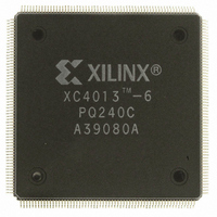
XC4013-6PQ240C Xilinx Inc, XC4013-6PQ240C Datasheet - Page 24

XC4013-6PQ240C
Manufacturer Part Number
XC4013-6PQ240C
Description
IC LOGIC CL ARRAY 13K GAT 240PQ
Manufacturer
Xilinx Inc
Series
XC4000r
Datasheet
1.XC4003-6PQ100C.pdf
(40 pages)
Specifications of XC4013-6PQ240C
Number Of Logic Elements/cells
1368
Number Of Labs/clbs
576
Total Ram Bits
18432
Number Of I /o
192
Number Of Gates
13000
Voltage - Supply
4.75 V ~ 5.25 V
Mounting Type
Surface Mount
Operating Temperature
0°C ~ 85°C
Package / Case
240-BFQFP
Lead Free Status / RoHS Status
Contains lead / RoHS non-compliant
Other names
122-1074
Available stocks
Company
Part Number
Manufacturer
Quantity
Price
LENGTH COUNT
Figure 22. Start-up Logic
XC4000, XC4000A, XC4000H Logic Cell Array Families
All Xilinx FPGAs of the XC2000, XC3000, XC4000 familiies
use a compatible bitstream format and can, therefore, be
connected in a daisy-chain in an arbitrary sequence. There
is however one limitation. The lead device must belong to
the highest family in the chain. If the chain contains
XC4000 devices, the master cannot be an XC2000 or
XC3000 device; if the daisy-chain contains XC3000 de-
vices, the master cannot be an XC2000 device. The
reason for this rule is shown in Figure 21 on the previous
page. Since all devices in the chain store the same length
count value and generate or receive one common se-
quence of CCLK pulses, they all recognize length-count
match on the same CCLK edge, as indicated on the left
edge of Figure 21. The master device will then drive
additional CCLK pulses until it reaches its finish point F.
The different families generate or require different num-
bers of additional CCLK pulses until they reach F.
Not reaching F means that the device does not really finish
its configuration, although DONE may have gone High, the
CLEAR MEMORY
STARTUP.CLK
STARTUP
USER NET
FULL
CCLK
Q3
Q2
*
*
*
S
K
Q
Q0
0
1
M
*
0
DONE
IN
1
Q1/Q4
1
0
0
1
*
D
K
CONFIGURATION BIT OPTIONS SELECTED BY USER IN "MAKEBITS "
Q
Q1
Q1
GSR ENABLE
GSR INVERT
STARTUP.GSR
STARTUP.GTS
GTS INVERT
GTS ENABLE
D
K
Q
Q2
*
*
*
*
CONTROLLED BY STARTUP SYMBOL
IN THE USER SCHEMATIC (SEE
LIBRARIES GUIDE)
USER NET
2-30
USER NET
0
1
1
0
M
*
outputs became active, and the internal RESET was
released. The user has some control over the relative
timing of these events and can, therefore, make sure that
they occur early enough.
But, for XC4000, not reaching F means that READBACK
cannot be initiated and most Boundary Scan instructions
cannot be used.This limitation has been critized by design-
ers who want to use an inexpensive lead device in periph-
eral mode and have the more precious I/O pins of the
XC4000 devices all available for user I/O. Here is a
solution for that case.
One CLB and one IOB in the lead XC3000 device are used
to generate the additional CCLK pulse required by the
XC4000 devices. When the lead device removes the
internal RESET signal, the 2-bit shift register responds to
its clock input and generates an active Low output signal
for the duration of the subsequent clock period. An exter-
nal connection between this output and CCLK thus creates
Q
D
K
R
S
Q
Q3
IOBs OPERATIONAL PER CONFIGURATION
GLOBAL SET/RESET OF
ALL CLB AND IOB FLIP-FLOPS
GLOBAL 3-STATE OF ALL IOBs
D
K
Q
Q4
1
0
" FINISHED "
ENABLES BOUNDARY
SCAN, READBACK AND
CONTROLS THE OSCILLATOR
DONE
X1528


