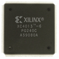
XC4013-6PQ240C Xilinx Inc, XC4013-6PQ240C Datasheet - Page 6

XC4013-6PQ240C
Manufacturer Part Number
XC4013-6PQ240C
Description
IC LOGIC CL ARRAY 13K GAT 240PQ
Manufacturer
Xilinx Inc
Series
XC4000r
Datasheet
1.XC4003-6PQ100C.pdf
(40 pages)
Specifications of XC4013-6PQ240C
Number Of Logic Elements/cells
1368
Number Of Labs/clbs
576
Total Ram Bits
18432
Number Of I /o
192
Number Of Gates
13000
Voltage - Supply
4.75 V ~ 5.25 V
Mounting Type
Surface Mount
Operating Temperature
0°C ~ 85°C
Package / Case
240-BFQFP
Lead Free Status / RoHS Status
Contains lead / RoHS non-compliant
Other names
122-1074
Available stocks
Company
Part Number
Manufacturer
Quantity
Price
XC4000, XC4000A, XC4000H Logic Cell Array Families
up/down counter, this means twice the speed in half the
number of CLBs, compared with the XC3000 families.
Pipelining Speeds Up The System: The abundance of
flip-flops in the CLBs invites pipelined designs. This is a
powerful way of increasing performance by breaking the
function into smaller subfunctions and executing them
in parallel, passing on the results through pipeline flip-
flops. This method should be seriously considered wher-
ever total performance is more important than simple
through-delay.
Wide Edge Decoding: For years, FPGAs have suffered
from the lack of wide decoding circuitry. When the address
or data field is wider than the function generator inputs (five
bits in the XC3000 families), FPGAs need multi-level
decoding and are thus slower than PALs. The XC4000-
family CLBs have nine inputs; any decoder of up to nine
inputs is, therefore, compact and fast. But, there is also a
need for much wider decoders, especially for address
decoding in large microprocessor systems. The XC4000
family has four programmable decoders located on each
edge of each device. Each of these wired-AND gates is
capable of accepting up to 42 inputs on the XC4005 and 72
on the XC4013. These decoders may also be split in two
when a large number of narrower decoders are required
for a maximum of 32 per device. These dedicated decod-
ers accept I/O signals and internal signals as inputs and
generate a decoded internal signal in 18 ns, pin-to-pin. The
XC4000A family has only two decoder AND gates per
edge which, when split provide a maximum of 16 per
device. Very large PALs can be emulated by ORing the
Figure 2. Fast Carry Logic in Each CLB
CIN 1
CIN 2
A1
B1
B0
A0
G4
G3
G2
G1
F4
F3
F2
F1
M
Carry
Logic
Carry
Logic
of G1 - G4
of F1 - F4
Function
Function
Logic
Logic
G'
F'
COUT
SUM 1
SUM 0
X5373
2-12
decoder outputs in a CLB. This decoding feature covers
what has long been considered a weakness of FPGAs.
Users often resorted to external PALs for simple but fast
decoding functions. Now, the dedicated decoders in the
XC4000 can implement these functions efficiently and
fast.
Higher Output Current: The 4-mA maximum output
current specification of today’s FPGAs often forces the
user to add external buffers, cumbersome especially on
bidirectional I/O lines. The XC4000 families solve many of
these problems by increasing the maximum output sink
current to 12 mA. Two adjacent outputs may be intercon-
nected to increase the output sink current to 24 mA. The
FPGA can thus drive short buses on a pc board. The
XC4000A and XC4000H outputs can sink 24 mA per
output and can double up for 48 mA.
While the XC2000 and XC3000 families used complemen-
tary output transistors, the XC4000 outputs are n-channel
for both pull-down and pull-up, somewhat analogous to the
classical totem pole used in TTL. The reduced output High
level (VOH) makes circuit delays more symmetrical for
TTL-threshold systems. The XC4000H outputs have an
optional p-channel output transistor.
Abundant Routing Resources
Connections between blocks are made by metal lines with
programmable switching points and switching matrices.
Compared to the previous LCA families, these routing
resources have been increased dramatically.The number
of globally distributed signals has been increased from two
to eight, and these lines have access to any clock or logic
input. The designer of synchronous systems can now
distribute not only several clocks, but also control signals,
all over the chip, without having to worry about any skew.
There are more than twice as many horizontal and vertical
Longlines that can carry signals across the length or width
of the chip with minimal delay and negligible skew.The
horizontal Longlines can be driven by 3-state buffers, and
can thus be used as unidirectional or bidirectional data
buses; or they can implement wide multiplexers or wired-
AND functions.
Single-length lines connect the switching matrices that are
located at every intersection of a row and a column of
CLBs. These lines provide the greatest interconnect flexi-
bility, but cause a delay whenever they go through a
switching matrix. Double-length lines bypass every other
matrix, and provide faster signal routing over intermediate
distances.
Compared to the XC3000 family, the XC4000 families
have more than double the routing resources, and they are
arranged in a far more regular fashion. In older devices,


