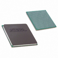
EP1SGX25CF672C7 Altera, EP1SGX25CF672C7 Datasheet - Page 253

EP1SGX25CF672C7
Manufacturer Part Number
EP1SGX25CF672C7
Description
IC STRATIX GX FPGA 25KLE 672FBGA
Manufacturer
Altera
Series
Stratix® GXr
Datasheet
1.EP1SGX10CF672C7N.pdf
(272 pages)
Specifications of EP1SGX25CF672C7
Number Of Logic Elements/cells
25660
Number Of Labs/clbs
2566
Total Ram Bits
1944576
Number Of I /o
455
Voltage - Supply
1.425 V ~ 1.575 V
Mounting Type
Surface Mount
Operating Temperature
0°C ~ 85°C
Package / Case
672-FBGA
Family Name
Stratix GX
Number Of Logic Blocks/elements
25660
# I/os (max)
455
Frequency (max)
4.38597GHz
Process Technology
SRAM
Operating Supply Voltage (typ)
1.5V
Logic Cells
25660
Ram Bits
1944576
Operating Supply Voltage (min)
1.425V
Operating Supply Voltage (max)
1.575V
Operating Temp Range
0C to 85C
Operating Temperature Classification
Commercial
Mounting
Surface Mount
Pin Count
672
Package Type
FC-FBGA
Lead Free Status / RoHS Status
Contains lead / RoHS non-compliant
Number Of Gates
-
Lead Free Status / Rohs Status
Not Compliant
Available stocks
Company
Part Number
Manufacturer
Quantity
Price
Part Number:
EP1SGX25CF672C7
Manufacturer:
ALTERA/阿尔特拉
Quantity:
20 000
- Current page: 253 of 272
- Download datasheet (3Mb)
Altera Corporation
June 2006
Decrease input delay to
internal cells
Decrease input delay to
input register
Decrease input delay to
output register
Increase delay to output
pin
Increase delay to output
enable pin
Increase output clock
enable delay
Increase input clock enable
delay
Increase output enable
clock enable delay
Table 6–78. Stratix GX IOE Programmable Delays on Column Pins
Parameter
Off
On
Small
Medium
Large
Off
On
Off
On
Off
On
Off
On
Off
On
Small
Large
Off
On
Small
Large
Off
On
Small
Large
Tables 6–78
programmable delays, respectively. These delays are controlled with the
Quartus II software logic options listed in the Parameter column.
Setting
-5 Speed Grade
and
Min
6–79
3,970
3,390
2,810
1,240
1,016
1,016
1,016
1,016
1,016
1,016
3900
show the adder delays for the column and row IOE
Max
212
212
377
338
540
540
540
0
0
0
0
0
0
0
-6 Speed Grade
Min
Stratix GX Device Handbook, Volume 1
4,367
3,729
3,091
4,290
1,364
1,118
1,118
1,118
1,118
1,118
1,118
Max
224
224
397
372
594
594
594
0
0
0
0
0
0
0
DC & Switching Characteristics
-7 Speed Grade
Min
5,022
4,288
3,554
4,933
1,568
1,285
1,285
1,285
1,285
1,285
1,285
Max
257
257
456
427
683
683
683
0
0
0
0
0
0
0
Unit
6–51
ps
ps
ps
ps
ps
ps
ps
ps
ps
ps
ps
ps
ps
ps
ps
ps
ps
ps
ps
ps
ps
ps
ps
ps
ps
Related parts for EP1SGX25CF672C7
Image
Part Number
Description
Manufacturer
Datasheet
Request
R

Part Number:
Description:
CYCLONE II STARTER KIT EP2C20N
Manufacturer:
Altera
Datasheet:

Part Number:
Description:
CPLD, EP610 Family, ECMOS Process, 300 Gates, 16 Macro Cells, 16 Reg., 16 User I/Os, 5V Supply, 35 Speed Grade, 24DIP
Manufacturer:
Altera Corporation
Datasheet:

Part Number:
Description:
CPLD, EP610 Family, ECMOS Process, 300 Gates, 16 Macro Cells, 16 Reg., 16 User I/Os, 5V Supply, 15 Speed Grade, 24DIP
Manufacturer:
Altera Corporation
Datasheet:

Part Number:
Description:
Manufacturer:
Altera Corporation
Datasheet:

Part Number:
Description:
CPLD, EP610 Family, ECMOS Process, 300 Gates, 16 Macro Cells, 16 Reg., 16 User I/Os, 5V Supply, 30 Speed Grade, 24DIP
Manufacturer:
Altera Corporation
Datasheet:

Part Number:
Description:
High-performance, low-power erasable programmable logic devices with 8 macrocells, 10ns
Manufacturer:
Altera Corporation
Datasheet:

Part Number:
Description:
High-performance, low-power erasable programmable logic devices with 8 macrocells, 7ns
Manufacturer:
Altera Corporation
Datasheet:

Part Number:
Description:
Classic EPLD
Manufacturer:
Altera Corporation
Datasheet:

Part Number:
Description:
High-performance, low-power erasable programmable logic devices with 8 macrocells, 10ns
Manufacturer:
Altera Corporation
Datasheet:

Part Number:
Description:
Manufacturer:
Altera Corporation
Datasheet:

Part Number:
Description:
Manufacturer:
Altera Corporation
Datasheet:

Part Number:
Description:
Manufacturer:
Altera Corporation
Datasheet:

Part Number:
Description:
CPLD, EP610 Family, ECMOS Process, 300 Gates, 16 Macro Cells, 16 Reg., 16 User I/Os, 5V Supply, 25 Speed Grade, 24DIP
Manufacturer:
Altera Corporation
Datasheet:


