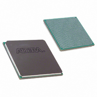
EP1SGX25CF672C7 Altera, EP1SGX25CF672C7 Datasheet - Page 72

EP1SGX25CF672C7
Manufacturer Part Number
EP1SGX25CF672C7
Description
IC STRATIX GX FPGA 25KLE 672FBGA
Manufacturer
Altera
Series
Stratix® GXr
Datasheet
1.EP1SGX10CF672C7N.pdf
(272 pages)
Specifications of EP1SGX25CF672C7
Number Of Logic Elements/cells
25660
Number Of Labs/clbs
2566
Total Ram Bits
1944576
Number Of I /o
455
Voltage - Supply
1.425 V ~ 1.575 V
Mounting Type
Surface Mount
Operating Temperature
0°C ~ 85°C
Package / Case
672-FBGA
Family Name
Stratix GX
Number Of Logic Blocks/elements
25660
# I/os (max)
455
Frequency (max)
4.38597GHz
Process Technology
SRAM
Operating Supply Voltage (typ)
1.5V
Logic Cells
25660
Ram Bits
1944576
Operating Supply Voltage (min)
1.425V
Operating Supply Voltage (max)
1.575V
Operating Temp Range
0C to 85C
Operating Temperature Classification
Commercial
Mounting
Surface Mount
Pin Count
672
Package Type
FC-FBGA
Lead Free Status / RoHS Status
Contains lead / RoHS non-compliant
Number Of Gates
-
Lead Free Status / Rohs Status
Not Compliant
Available stocks
Company
Part Number
Manufacturer
Quantity
Price
Part Number:
EP1SGX25CF672C7
Manufacturer:
ALTERA/阿尔特拉
Quantity:
20 000
Logic Elements
Figure 4–5. LE in Normal Mode
Note to
(1)
4–6
Stratix GX Device Handbook, Volume 1
This signal is only allowed in normal mode if the LE is at the end of an adder/subtractor chain.
Figure
addnsub (LAB Wide)
data1
data2
data3
cin (from cout
of previous LE)
data4
4–5:
(1)
clock enable control for the register. These LAB-wide signals are available
in all LE modes. The addnsub control signal is allowed in arithmetic
mode.
The Quartus II software, in conjunction with parameterized functions
such as library of parameterized modules (LPM) functions, automatically
chooses the appropriate mode for common functions such as counters,
adders, subtractors, and arithmetic functions. If required, you can also
create special-purpose functions that specify which LE operating mode to
use for optimal performance.
Normal Mode
The normal mode is suitable for general logic applications and
combinatorial functions. In normal mode, four data inputs from the LAB
local interconnect are inputs to a four-input LUT (see
Quartus II Compiler automatically selects the carry-in or the data3
signal as one of the inputs to the LUT. Each LE can use LUT chain
connections to drive its combinatorial output directly to the next LE in the
LAB. Asynchronous load data for the register comes from the data3
input of the LE. LEs in normal mode support packed registers.
Register Feedback
4-Input
LUT
Register chain
connection
clock (LAB Wide)
(LAB Wide)
ena (LAB Wide)
aclr (LAB Wide)
sload
(LAB Wide)
sclear
(LAB Wide)
ADATA
ENA
D
ALD/PRE
aload
CLRN
Q
Row, column, and
direct link routing
Row, column, and
direct link routing
Local routing
LUT chain
connection
Register
chain output
Figure
Altera Corporation
February 2005
4–5). The


