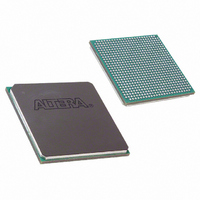
EP1SGX25DF672I6 Altera, EP1SGX25DF672I6 Datasheet - Page 162

EP1SGX25DF672I6
Manufacturer Part Number
EP1SGX25DF672I6
Description
IC STRATIX GX FPGA 25K 672-FBGA
Manufacturer
Altera
Series
Stratix® GXr
Datasheet
1.EP1SGX10CF672C7N.pdf
(272 pages)
Specifications of EP1SGX25DF672I6
Number Of Logic Elements/cells
25660
Number Of Labs/clbs
2566
Total Ram Bits
1944576
Number Of I /o
455
Voltage - Supply
1.425 V ~ 1.575 V
Mounting Type
Surface Mount
Operating Temperature
-40°C ~ 100°C
Package / Case
672-FBGA
Family Name
Stratix GX
Number Of Logic Blocks/elements
25660
# I/os (max)
455
Frequency (max)
5GHz
Process Technology
SRAM
Operating Supply Voltage (typ)
1.5V
Logic Cells
25660
Ram Bits
1944576
Operating Supply Voltage (min)
1.425V
Operating Supply Voltage (max)
1.575V
Operating Temp Range
-40C to 100C
Operating Temperature Classification
Industrial
Mounting
Surface Mount
Pin Count
672
Package Type
FC-FBGA
Lead Free Status / RoHS Status
Contains lead / RoHS non-compliant
Number Of Gates
-
Lead Free Status / Rohs Status
Not Compliant
Available stocks
Company
Part Number
Manufacturer
Quantity
Price
Company:
Part Number:
EP1SGX25DF672I6
Manufacturer:
ALTERA30
Quantity:
50
- Current page: 162 of 272
- Download datasheet (3Mb)
I/O Structure
I/O Structure
4–96
Stratix GX Device Handbook, Volume 1
Phase Shifting
Stratix GX device fast PLLs have advanced clock shift capability that
enables programmable phase shifts. You can enter a phase shift (in
degrees or time units) for each PLL clock output port or for all outputs
together in one shift. You can perform phase shifting in time units with a
resolution range of 150 to 400 ps. This resolution is a function of the VCO
period.
Control Signals
The fast PLL has the same lock output, pllenable input, and areset
input control signals as the enhanced PLL.
For more information on high-speed differential I/O support, see the
High-Speed Source-Synchronous Differential I/O Interfaces in Stratix GX
Devices chapter of the Stratix GX Device Handbook, Volume 2.
IOEs provide many features, including:
■
■
■
■
■
■
■
■
■
■
■
■
■
■
■
The IOE in Stratix GX devices contains a bidirectional I/O buffer, six
registers, and a latch for a complete embedded bidirectional single data
rate or DDR transfer.
IOE contains two input registers (plus a latch), two output registers, and
two output enable registers. The design can use both input registers and
the latch to capture DDR input and both output registers to drive DDR
outputs. Additionally, the design can use the output enable (OE) register
for fast clock-to-output enable timing. The negative edge-clocked OE
register is used for DDR SDRAM interfacing. The Quartus II software
automatically duplicates a single OE register that controls multiple
output or bidirectional pins.
Dedicated differential and single-ended I/O buffers
3.3-V, 64-bit, 66-MHz PCI compliance
3.3-V, 64-bit, 133-MHz PCI-X 1.0 compliance
Joint Test Action Group (JTAG) boundary-scan test (BST) support
Differential on-chip termination for LVDS I/O standard
Programmable pull-up during configuration
Output drive strength control
Slew-rate control
Tri-state buffers
Bus-hold circuitry
Programmable pull-up resistors
Programmable input and output delays
Open-drain outputs
DQ and DQS I/O pins
Double-data rate (DDR) Registers
Figure 4–58
shows the Stratix GX IOE structure. The
Altera Corporation
February 2005
Related parts for EP1SGX25DF672I6
Image
Part Number
Description
Manufacturer
Datasheet
Request
R

Part Number:
Description:
Stratix Gx Device Family Data Sheet
Manufacturer:
Altera Corporation
Datasheet:

Part Number:
Description:
CYCLONE II STARTER KIT EP2C20N
Manufacturer:
Altera
Datasheet:

Part Number:
Description:
CPLD, EP610 Family, ECMOS Process, 300 Gates, 16 Macro Cells, 16 Reg., 16 User I/Os, 5V Supply, 35 Speed Grade, 24DIP
Manufacturer:
Altera Corporation
Datasheet:

Part Number:
Description:
CPLD, EP610 Family, ECMOS Process, 300 Gates, 16 Macro Cells, 16 Reg., 16 User I/Os, 5V Supply, 15 Speed Grade, 24DIP
Manufacturer:
Altera Corporation
Datasheet:

Part Number:
Description:
Manufacturer:
Altera Corporation
Datasheet:

Part Number:
Description:
CPLD, EP610 Family, ECMOS Process, 300 Gates, 16 Macro Cells, 16 Reg., 16 User I/Os, 5V Supply, 30 Speed Grade, 24DIP
Manufacturer:
Altera Corporation
Datasheet:

Part Number:
Description:
High-performance, low-power erasable programmable logic devices with 8 macrocells, 10ns
Manufacturer:
Altera Corporation
Datasheet:

Part Number:
Description:
High-performance, low-power erasable programmable logic devices with 8 macrocells, 7ns
Manufacturer:
Altera Corporation
Datasheet:

Part Number:
Description:
Classic EPLD
Manufacturer:
Altera Corporation
Datasheet:

Part Number:
Description:
High-performance, low-power erasable programmable logic devices with 8 macrocells, 10ns
Manufacturer:
Altera Corporation
Datasheet:

Part Number:
Description:
Manufacturer:
Altera Corporation
Datasheet:

Part Number:
Description:
Manufacturer:
Altera Corporation
Datasheet:

Part Number:
Description:
Manufacturer:
Altera Corporation
Datasheet:


