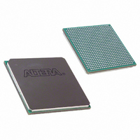
EP1SGX25DF672I6 Altera, EP1SGX25DF672I6 Datasheet - Page 63

EP1SGX25DF672I6
Manufacturer Part Number
EP1SGX25DF672I6
Description
IC STRATIX GX FPGA 25K 672-FBGA
Manufacturer
Altera
Series
Stratix® GXr
Datasheet
1.EP1SGX10CF672C7N.pdf
(272 pages)
Specifications of EP1SGX25DF672I6
Number Of Logic Elements/cells
25660
Number Of Labs/clbs
2566
Total Ram Bits
1944576
Number Of I /o
455
Voltage - Supply
1.425 V ~ 1.575 V
Mounting Type
Surface Mount
Operating Temperature
-40°C ~ 100°C
Package / Case
672-FBGA
Family Name
Stratix GX
Number Of Logic Blocks/elements
25660
# I/os (max)
455
Frequency (max)
5GHz
Process Technology
SRAM
Operating Supply Voltage (typ)
1.5V
Logic Cells
25660
Ram Bits
1944576
Operating Supply Voltage (min)
1.425V
Operating Supply Voltage (max)
1.575V
Operating Temp Range
-40C to 100C
Operating Temperature Classification
Industrial
Mounting
Surface Mount
Pin Count
672
Package Type
FC-FBGA
Lead Free Status / RoHS Status
Contains lead / RoHS non-compliant
Number Of Gates
-
Lead Free Status / Rohs Status
Not Compliant
Available stocks
Company
Part Number
Manufacturer
Quantity
Price
Company:
Part Number:
EP1SGX25DF672I6
Manufacturer:
ALTERA30
Quantity:
50
- Current page: 63 of 272
- Download datasheet (3Mb)
Altera Corporation
August 2005
Figure 3–10. Misaligned Captured Bits
The dynamic phase selector and synchronizer align the clock and data
based on the power-up of both communicating devices, and the channel
to channel skew. However, the dynamic phase selector and synchronizer
cannot determine the byte boundary, and the data may need to be
byte-aligned. The dynamic phase aligner’s data realignment circuitry
shifts data bits to correct bit misalignments.
The Stratix GX circuitry contains a data-realignment feature controlled by
the logic array. Stratix GX devices perform data realignment on the
parallel data after the deserialization block. The data realignment can be
performed per channel for more flexibility. The data alignment operation
requires a state machine to recognize a specific pattern. The procedure
requires the bits to be slipped on the data stream to correctly align the
incoming data to the start of the byte boundary.
The DPA uses its realignment circuitry and the global clock for data
realignment. Either a device pin or the logic array asserts the internal
rx_channel_data_align node to activate the DPA data-realignment
circuitry. Switching this node from low to high activates the realignment
circuitry and the data being transferred to the logic array is shifted by
one bit. The data realignment block cannot be bypassed. However, if the
rx_channel_data_align is not turned on (through the altvlds
MegaWizard Plug-In Manager), or when it is not toggled, it only acts as a
register latency.
A state machine and additional logic can monitor the incoming parallel
data and compare it against a known pattern. If the incoming data pattern
does not match the known pattern, you can activate the
rx_channel_data_align node again. Repeat this process until the
realigner detects the desired match between the known data pattern and
incoming parallel data pattern.
Correct Alignment
Incorrect Alignment
0
3
1
4
2
5
Source-Synchronous Signaling With DPA
3
6
Stratix GX Device Handbook, Volume 1
4
7
5
0
6
1
7
2
3–13
Related parts for EP1SGX25DF672I6
Image
Part Number
Description
Manufacturer
Datasheet
Request
R

Part Number:
Description:
Stratix Gx Device Family Data Sheet
Manufacturer:
Altera Corporation
Datasheet:

Part Number:
Description:
CYCLONE II STARTER KIT EP2C20N
Manufacturer:
Altera
Datasheet:

Part Number:
Description:
CPLD, EP610 Family, ECMOS Process, 300 Gates, 16 Macro Cells, 16 Reg., 16 User I/Os, 5V Supply, 35 Speed Grade, 24DIP
Manufacturer:
Altera Corporation
Datasheet:

Part Number:
Description:
CPLD, EP610 Family, ECMOS Process, 300 Gates, 16 Macro Cells, 16 Reg., 16 User I/Os, 5V Supply, 15 Speed Grade, 24DIP
Manufacturer:
Altera Corporation
Datasheet:

Part Number:
Description:
Manufacturer:
Altera Corporation
Datasheet:

Part Number:
Description:
CPLD, EP610 Family, ECMOS Process, 300 Gates, 16 Macro Cells, 16 Reg., 16 User I/Os, 5V Supply, 30 Speed Grade, 24DIP
Manufacturer:
Altera Corporation
Datasheet:

Part Number:
Description:
High-performance, low-power erasable programmable logic devices with 8 macrocells, 10ns
Manufacturer:
Altera Corporation
Datasheet:

Part Number:
Description:
High-performance, low-power erasable programmable logic devices with 8 macrocells, 7ns
Manufacturer:
Altera Corporation
Datasheet:

Part Number:
Description:
Classic EPLD
Manufacturer:
Altera Corporation
Datasheet:

Part Number:
Description:
High-performance, low-power erasable programmable logic devices with 8 macrocells, 10ns
Manufacturer:
Altera Corporation
Datasheet:

Part Number:
Description:
Manufacturer:
Altera Corporation
Datasheet:

Part Number:
Description:
Manufacturer:
Altera Corporation
Datasheet:

Part Number:
Description:
Manufacturer:
Altera Corporation
Datasheet:


