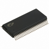
CY7C68013-56PVC Cypress Semiconductor Corp, CY7C68013-56PVC Datasheet - Page 11

CY7C68013-56PVC
Manufacturer Part Number
CY7C68013-56PVC
Description
IC MCU USB PERIPH HI SPD 56SSOP
Manufacturer
Cypress Semiconductor Corp
Series
EZ-USB FX2LP™r
Datasheet
1.CY7C68013-56PVC.pdf
(52 pages)
Specifications of CY7C68013-56PVC
Applications
USB Microcontroller
Core Processor
8051
Program Memory Type
ROMless
Controller Series
CY7C680xx
Ram Size
16K x 8
Interface
I²C, USB, USART
Number Of I /o
24
Voltage - Supply
3 V ~ 3.6 V
Operating Temperature
0°C ~ 70°C
Mounting Type
Surface Mount
Package / Case
56-SSOP
Lead Free Status / RoHS Status
Contains lead / RoHS non-compliant
Other names
428-1332
Available stocks
Company
Part Number
Manufacturer
Quantity
Price
Company:
Part Number:
CY7C68013-56PVC
Manufacturer:
CY
Quantity:
5 530
Company:
Part Number:
CY7C68013-56PVC
Manufacturer:
CY
Quantity:
6 100
Part Number:
CY7C68013-56PVC
Manufacturer:
CYPRESS/赛普拉斯
Quantity:
20 000
If Autovectoring is enabled (AV2EN = 1 in the INTSETUP register), the FX2 substitutes its INT2VEC byte. Therefore, if the high
byte (“page”) of a jump-table address is preloaded at location 0x0044, the automatically-inserted INT2VEC byte at 0x0045 will
direct the jump to the correct address out of the 27 addresses within the page.
3.8.3
Just as the USB Interrupt is shared among 27 individual USB-interrupt sources, the FIFO/GPIF interrupt is shared among 14
individual FIFO/GPIF sources. The FIFO/GPIF Interrupt, like the USB Interrupt, can employ autovectoring. Table 3-4 shows the
priority and INT4VEC values for the 14 FIFO/GPIF interrupt sources
Table 3-4. Individual FIFO/GPIF Interrupt Sources
If Autovectoring is enabled (AV4EN = 1 in the INTSETUP register), the FX2 substitutes its INT4VEC byte. Therefore, if the high
byte (“page”) of a jump-table address is preloaded at location 0x0054, the automatically-inserted INT4VEC byte at 0x0055 will
direct the jump to the correct address out of the 14 addresses within the page. When the ISR occurs, the FX2 pushes the program
counter onto its stack then jumps to address 0x0053, where it expects to find a “jump” instruction to the ISR Interrupt service
routine.
3.9
3.9.1
An input pin (RESET#) resets the chip. This pin has hysteresis and is active LOW. The internal PLL stabilizes approximately 200
3.9.2
The 8051 puts itself and the rest of the chip into a power-down mode by setting PCON.0 = 1. This stops the oscillator and PLL.
When WAKEUP is asserted by external logic, the oscillator restarts and after the PLL stabilizes, and the 8051 receives a wakeup
interrupt. This applies whether or not FX2 is connected to the USB.
The FX2 exits the power down (USB suspend) state using one of the following methods:
The second wakeup pin, WU2, can also be configured as a general purpose I/O pin. This allows a simple external R-C network
to be used as a periodic wakeup source.
3.10
3.10.1
The FX2 has eight kbytes of internal program/data RAM, where PSEN#/RD# signals are internally ORed to allow the 8051 to
access it as both program and data memory. No USB control registers appear in this space.
Document #: 38-08012 Rev. *C
• USB bus signals resume
• External logic asserts the WAKEUP pin
• External logic asserts the PA3/WU2 pin.
s after V
Priority
10
11
12
13
14
1
2
3
4
5
6
7
8
9
FIFO/GPIF Interrupt (INT4)
Reset and Wakeup
Reset Pin
Wakeup Pins
Program/Data RAM
Size
CC
has reached 3.3V. Typically, an external RC network (R = 100k, C = 0.1 F) is used to provide the RESET# signal.
INT4VEC Value
AC
8C
9C
A0
A4
80
88
90
94
98
A8
B0
B4
84
GPIFDONE
GPIFWF
Source
EP2PF
EP4PF
EP6PF
EP8PF
EP2EF
EP4EF
EP6EF
EP8EF
EP2FF
EP4FF
EP6FF
EP8FF
Endpoint 2 Programmable Flag
Endpoint 4 Programmable Flag
Endpoint 6 Programmable Flag
Endpoint 8 Programmable Flag
Endpoint 2 Empty Flag
Endpoint 4 Empty Flag
Endpoint 6 Empty Flag
Endpoint 8 Empty Flag
Endpoint 2 Full Flag
Endpoint 4 Full Flag
Endpoint 6 Full Flag
Endpoint 8 Full Flag
GPIF Operation Complete
GPIF Waveform
Notes
CY7C68013
Page 11 of 52


