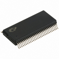
CY7C68013-56PVC Cypress Semiconductor Corp, CY7C68013-56PVC Datasheet - Page 17

CY7C68013-56PVC
Manufacturer Part Number
CY7C68013-56PVC
Description
IC MCU USB PERIPH HI SPD 56SSOP
Manufacturer
Cypress Semiconductor Corp
Series
EZ-USB FX2LP™r
Datasheet
1.CY7C68013-56PVC.pdf
(52 pages)
Specifications of CY7C68013-56PVC
Applications
USB Microcontroller
Core Processor
8051
Program Memory Type
ROMless
Controller Series
CY7C680xx
Ram Size
16K x 8
Interface
I²C, USB, USART
Number Of I /o
24
Voltage - Supply
3 V ~ 3.6 V
Operating Temperature
0°C ~ 70°C
Mounting Type
Surface Mount
Package / Case
56-SSOP
Lead Free Status / RoHS Status
Contains lead / RoHS non-compliant
Other names
428-1332
Available stocks
Company
Part Number
Manufacturer
Quantity
Price
Company:
Part Number:
CY7C68013-56PVC
Manufacturer:
CY
Quantity:
5 530
Company:
Part Number:
CY7C68013-56PVC
Manufacturer:
CY
Quantity:
6 100
Part Number:
CY7C68013-56PVC
Manufacturer:
CYPRESS/赛普拉斯
Quantity:
20 000
The GPIF has six programmable control outputs (CTL), nine address outputs (GPIFADRx), and six general-purpose ready inputs
(RDY). The data bus width can be 8 or 16 bits. Each GPIF vector defines the state of the control outputs, and determines what
state a ready input (or multiple inputs) must be before proceeding. The GPIF vector can be programmed to advance a FIFO to
the next data value, advance an address, etc. A sequence of the GPIF vectors make up a single waveform that will be executed
to perform the desired data move between the CY7C68013 and the external design.
3.14.1
The 100- and 128-pin packages bring out all six Control Output pins (CTL0-CTL5). The 8051 programs the GPIF unit to define
the CTL waveforms. The 56-pin package brings out three of these signals, CTL0–CTL2. CTLx waveform edges can be
programmed to make transitions as fast as once per clock (20.8 ns using a 48-MHz clock).
3.14.2
The 100- and 128-pin packages bring out all six Ready inputs (RDY0–RDY5). The 8051 programs the GPIF unit to test the RDY
pins for GPIF branching. The 56-pin package brings out two of these signals, RDY0–1.
3.14.3
Nine GPIF address lines are available in the 100- and 128-pin packages, GPIFADR[8..0]. The GPIF address lines allow indexing
through up to a 512-byte block of RAM. If more address lines are needed, I/O port pins can be used.
3.14.4
In master mode, the 8051 appropriately sets GPIF transaction count registers (GPIFTCB3, GPIFTCB2, GPIFTCB1, or
GPIFTCB0) for unattended transfers of up to 4,294,967,296 bytes. The GPIF automatically throttles data flow to prevent under
or overflow until the full number of requested transactions complete. The GPIF decrements the value in these registers to
represent the current status of the transaction.
3.15
The core has the ability to directly edit the data contents of the internal 8-kbyte RAM and of the internal 512-byte scratch pad
RAM via a vendor-specific command. This capability is normally used when “soft” downloading user code and is available only
to and from internal RAM, whether the 8051 is held in reset or running. The available RAM spaces are 8 kbytes from
0x0000–0x1FFF (code/data) and 512 bytes from 0xE000–0xE1FF (scratch pad RAM).
Note: A “loader” running in internal RAM can be used to transfer downloaded data to external memory.
3.16
FX2 provides two identical autopointers. They are similar to the internal 8051 data pointers, but with an additional feature: they
can optionally increment a pointer address after every memory access. This capability is available to and from both internal and
external RAM. The autopointers are available in external FX2 registers, under control of a mode bit (AUTOPTRSETUP.0). Using
the external FX2 autopointer access (at 0xE67B – 0xE67C) allows the autopointer to access all RAM, internal and external to
the part. Also, the autopointers can point to any FX2 register or endpoint buffer space. When autopointer access to external
memory is enabled, location 0xE67B and 0xE67C in XDATA and PDATA space cannot be used.
3.17
FX2 has one I
VID/PID/DID and configuration information, and another that the 8051, once running, uses to control external I
devices. The I
3.17.1
The I
be configured properly. See Table 3-7 for configuring the device address pins.
Document #: 38-08012 Rev. *C
2
C-compatible pins SCL and SDA must have external 2.2-k pull-up resistors. External EEPROM device address pins must
Six Control OUT Signals
Six Ready IN Signals
Nine GPIF Address OUT signals
Long Transfer Mode
USB Uploads and Downloads
Autopointer Access
I
I
2
2
C-compatible Port Pins
C-compatible Controller
2
2
C-compatible port operates in master mode only.
C-compatible port that is driven by two internal controllers, one that automatically operates at boot time to load
CY7C68013
2
Page 17 of 52
C-compatible


