CY7C68013-56PVC Cypress Semiconductor Corp, CY7C68013-56PVC Datasheet - Page 26
CY7C68013-56PVC
Manufacturer Part Number
CY7C68013-56PVC
Description
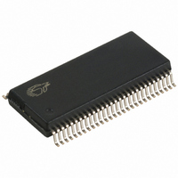
IC MCU USB PERIPH HI SPD 56SSOP
Manufacturer
Cypress Semiconductor Corp
Series
EZ-USB FX2LP™r
Datasheet
1.CY7C68013-56PVC.pdf
(52 pages)
Specifications of CY7C68013-56PVC
Applications
USB Microcontroller
Core Processor
8051
Program Memory Type
ROMless
Controller Series
CY7C680xx
Ram Size
16K x 8
Interface
I²C, USB, USART
Number Of I /o
24
Voltage - Supply
3 V ~ 3.6 V
Operating Temperature
0°C ~ 70°C
Mounting Type
Surface Mount
Package / Case
56-SSOP
Lead Free Status / RoHS Status
Contains lead / RoHS non-compliant
Other names
428-1332
Available stocks
Company
Part Number
Manufacturer
Quantity
Price
Company:

Part Number:
CY7C68013-56PVC
Manufacturer:
CY
Quantity:
5 530
Company:
Part Number:
CY7C68013-56PVC
Manufacturer:
CY
Quantity:
6 100
Part Number:
CY7C68013-56PVC
Manufacturer:
CYPRESS/赛普拉斯
Quantity:
20 000


Table 4-1. FX2 Pin Descriptions (continued)
Document #: 38-08012 Rev. *C
TQFP
Port B
PORT C
128
92
44
45
46
47
54
55
56
57
72
73
74
75
76
TQFP
100
74
34
35
36
37
44
45
46
47
57
58
59
60
61
SSOP
56
47
25
26
27
28
29
30
31
32
QFN
56
40 PA7 or
18 PB0 or
19 PB1 or
20 PB2 or
21 PB3 or
22 PB4 or
23 PB5 or
24 PB6 or
25 PB7 or
FLAGD or
SLCS#
FD[0]
FD[1]
FD[2]
TXD1 or
FD[3]
FD[4]
FD[5]
FD[6]
FD[7]
PC0 or
GPIFADR0
PC1 or
GPIFADR1
PC2 or
GPIFADR2
PC3 or
GPIFADR3
PC4 or
GPIFADR4
Name
Type
I/O/Z
I/O/Z
I/O/Z
I/O/Z
I/O/Z
I/O/Z
I/O/Z
I/O/Z
I/O/Z
I/O/Z
I/O/Z
I/O/Z
I/O/Z
I/O/Z
[5]
Default
(PB0)
(PB1)
(PB2)
(PB3)
(PB4)
(PB5)
(PB6)
(PB7)
(PC0)
(PC1)
(PC2)
(PC3)
(PC4)
(PA7)
I
I
I
I
I
I
I
I
I
I
I
I
I
I
Multiplexed pin whose function is selected by the IFCONFIG[1:0]
and PORTACFG.7 bits.
PA7 is a bidirectional I/O port pin.
FLAGD is a programmable slave-FIFO output status flag signal.
SLCS# gates all other slave FIFO enable/strobes
Multiplexed pin whose function is selected by the following bits:
IFCONFIG[1..0].
PB0 is a bidirectional I/O port pin.
FD[0] is the bidirectional FIFO/GPIF data bus.
Multiplexed pin whose function is selected by the following bits:
IFCONFIG[1..0].
PB1 is a bidirectional I/O port pin.
FD[1] is the bidirectional FIFO/GPIF data bus.
Multiplexed pin whose function is selected by the following bits:
IFCONFIG[1..0].
PB2 is a bidirectional I/O port pin.
FD[2] is the bidirectional FIFO/GPIF data bus.
Multiplexed pin whose function is selected by the following bits:
IFCONFIG[1..0].
PB3 is a bidirectional I/O port pin.
FD[3] is the bidirectional FIFO/GPIF data bus.
Multiplexed pin whose function is selected by the following bits:
IFCONFIG[1..0].
PB4 is a bidirectional I/O port pin.
FD[4] is the bidirectional FIFO/GPIF data bus.
Multiplexed pin whose function is selected by the following bits:
IFCONFIG[1..0].
PB5 is a bidirectional I/O port pin.
FD[5] is the bidirectional FIFO/GPIF data bus.
Multiplexed pin whose function is selected by the following bits:
IFCONFIG[1..0].
PB6 is a bidirectional I/O port pin.
FD[6] is the bidirectional FIFO/GPIF data bus.
Multiplexed pin whose function is selected by the following bits:
IFCONFIG[1..0].
PB7 is a bidirectional I/O port pin.
FD[7] is the bidirectional FIFO/GPIF data bus.
Multiplexed pin whose function is selected by PORTCCFG.0
PC0 is a bidirectional I/O port pin.
GPIFADR0 is a GPIF address output pin.
Multiplexed pin whose function is selected by PORTCCFG.1
PC1 is a bidirectional I/O port pin.
GPIFADR1 is a GPIF address output pin.
Multiplexed pin whose function is selected by PORTCCFG.2
PC2 is a bidirectional I/O port pin.
GPIFADR2 is a GPIF address output pin.
Multiplexed pin whose function is selected by PORTCCFG.3
PC3 is a bidirectional I/O port pin.
GPIFADR3 is a GPIF address output pin.
Multiplexed pin whose function is selected by PORTCCFG.4
PC4 is a bidirectional I/O port pin.
GPIFADR4 is a GPIF address output pin.
Description
CY7C68013
Page 26 of 52
Related parts for CY7C68013-56PVC
Image
Part Number
Description
Manufacturer
Datasheet
Request
R

Part Number:
Description:
IC MCU USB PERIPH HI SPD 100LQFP
Manufacturer:
Cypress Semiconductor Corp
Datasheet:

Part Number:
Description:
IC MCU USB PERIPH HI SPD 56SSOP
Manufacturer:
Cypress Semiconductor Corp
Datasheet:
Part Number:
Description:
IC MCU USB PERIPH HI SPD 100LQFP
Manufacturer:
Cypress Semiconductor Corp
Datasheet:

Part Number:
Description:
Manufacturer:
Cypress Semiconductor Corp
Datasheet:
Part Number:
Description:
Manufacturer:
Cypress Semiconductor Corp
Datasheet:

Part Number:
Description:
Manufacturer:
Cypress Semiconductor Corp
Datasheet:
Part Number:
Description:
Manufacturer:
Cypress Semiconductor Corp
Datasheet:
Part Number:
Description:
Manufacturer:
Cypress Semiconductor Corp
Datasheet:
Part Number:
Description:
Manufacturer:
Cypress Semiconductor Corp
Datasheet: