PRIXP425BC Intel, PRIXP425BC Datasheet - Page 32
PRIXP425BC
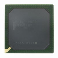
Manufacturer Part Number
PRIXP425BC
Description
IC NETWRK PROCESSR 400MHZ 492BGA
Manufacturer
Intel
Specifications of PRIXP425BC
Processor Type
Network
Features
XScale Core
Speed
400MHz
Voltage
1.3V
Mounting Type
Surface Mount
Package / Case
492-BGA
Core Operating Frequency
400MHz
Package Type
BGA
Pin Count
492
Mounting
Surface Mount
Operating Temperature (max)
70C
Operating Temperature (min)
0C
Operating Temperature Classification
Commercial
Lead Free Status / RoHS Status
Lead free / RoHS Compliant
Other names
869083
Available stocks
Company
Part Number
Manufacturer
Quantity
Price

Part Number:
PRIXP425BC
Manufacturer:
INTEL
Quantity:
20 000


Core Errata
Workaround:
Status:
6.
Problem:
Workaround:
Status:
7.
Problem:
Workaround:
Status:
8.
Problem:
32
The Intel XScale
register (opcode2 = 0b000) and the Cache Type register (opcode2 = 0b001). When any of the
unimplemented registers are accessed by software (for example, mrc p15, 0, r3, c15, c15, 2), the
value of the Main ID register was to be returned. Instead, an unpredictable value is returned.
No workaround.
No
Disabling and Re-Enabling the MMU can Hang the Core or Cause it to
Execute the Wrong Code
When the MMU is disabled via the CP15 control register (CP15, CR1, opcode_2 = 0, bit 0) after
being enabled, certain timing cases can cause the processor to hang. In addition to this, re-enabling
the MMU after disabling it can cause the processor to fetch and execute code from the wrong
physical address. To avoid these issues, the code sequence below must be used whenever disabling
the MMU or re-enabling it afterwards.
The following code sequence can be used to disable and/or re-enable the MMU safely. The
alignment of the mcr instruction that disables or re-enables the MMU must be controlled carefully
so that it resides in the first word of an instruction cache line.
@ The following code sequence takes r0 as a parameter. The value of r0 will be
@written to the CP15 control register to either enable or disable the MMU.
mcr p15, 0, r0, c10, c4, 1 @ unlock I-TLB
mcr p15, 0, r0, c8, c5, 0 @ invalidate I-TLB
mrc p15, 0, r0, c2, c0, 0 @ CPWAIT
mov r0, r0
sub pc, pc, #4
b 1f @ branch to aligned code
.align 5
1:
mcr p15, 0, r0, c1, c0, 0 @ enable/disable MMU, caches
mrc p15, 0, r0, c2, c0, 0 @ CPWAIT
mov r0, r0
sub pc, pc, #4
No
Updating the JTAG Parallel Registers Requires an Extra TCK Rising Edge
The IEEE 1149.1 spec states that the effects of updating all parallel JTAG registers should be seen
on the falling edge of TCK in the Update-DR state. The Intel XScale core parallel JTAG registers
require an extra TCK rising edge to make the update visible. Therefore, operations like hold-reset,
JTAG break, and vector traps require either an extra TCK cycle by going to Run-Test-Idle or by
cycling through the state machine again in order to trigger the expected hardware behavior.
When the JTAG interface is polled continuously, this erratum has no effect. When not, an extra
TCK cycle can be caused by going to Run-Test-Idle after writing a parallel JTAG register.
No Fix
Non-Branch Instruction in Vector Table May Execute Twice After a Thumb
Mode Exception
When an exception occurs in thumb mode and a non-branch instruction is executed at the corre-
sponding exception vector, that instruction may execute twice. Typically instructions located at
exception vectors must be branch instructions which go to the appropriate handler, but the ARM
Fix.
Fix.
Intel
®
IXP42X Product Line of Network Processors and IXC1100 Control Plane Processor
®
Core does not implement any CP15 ID code registers other than the Main ID
Related parts for PRIXP425BC
Image
Part Number
Description
Manufacturer
Datasheet
Request
R

Part Number:
Description:
Microprocessor: Intel Celeron M Processor 320 and Ultra Low Voltage Intel Celeron M Processor at 600MHz
Manufacturer:
Intel Corporation
Part Number:
Description:
Intel 82550 Fast Ethernet Multifunction PCI/CardBus Controller
Manufacturer:
Intel Corporation
Datasheet:
Part Number:
Description:
Intel StrataFlash memory 32 Mbit. Access speed 120 ns
Manufacturer:
Intel Corporation
Datasheet:
Part Number:
Description:
Intel StrataFlash memory 32 Mbit. Access speed 120 ns
Manufacturer:
Intel Corporation
Datasheet:
Part Number:
Description:
Intel StrataFlash memory 64 Mbit. Access speed 150 ns
Manufacturer:
Intel Corporation
Datasheet:
Part Number:
Description:
Intel StrataFlash memory 32 Mbit. Access speed 100 ns
Manufacturer:
Intel Corporation
Datasheet:
Part Number:
Description:
DA28F640J5A-1505 Volt Intel StrataFlash Memory
Manufacturer:
Intel Corporation
Datasheet:
Part Number:
Description:
5 Volt Intel StrataFlash?? Memory
Manufacturer:
Intel Corporation
Datasheet:
Part Number:
Description:
5 Volt Intel StrataFlash?? Memory
Manufacturer:
Intel Corporation
Part Number:
Description:
Intel 6300ESB I/O Controller Hub
Manufacturer:
Intel Corporation
Datasheet:
Part Number:
Description:
Intel 82801DB I/O Controller Hub (ICH4), Pb-Free SLI
Manufacturer:
Intel Corporation
Datasheet:
Part Number:
Description:
Intel 82801FB I/O Controller Hub (ICH6)
Manufacturer:
Intel Corporation
Datasheet:
Part Number:
Description:
Intel Strataflash Memory28F128J3 28F640J3 28F320J3
Manufacturer:
Intel Corporation
Datasheet:
Part Number:
Description:
Controllers, Intel 430TX PCIset: 82439TX System Controller (MTXC)
Manufacturer:
Intel Corporation