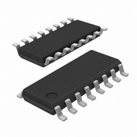
SI3000-C-FS Silicon Laboratories Inc, SI3000-C-FS Datasheet - Page 18

SI3000-C-FS
Manufacturer Part Number
SI3000-C-FS
Description
IC VOICE CODEC 3.3V/5V 16SOIC
Manufacturer
Silicon Laboratories Inc
Type
Voice-Band Codecr
Datasheet
1.SI3000-C-FS.pdf
(34 pages)
Specifications of SI3000-C-FS
Package / Case
16-SOIC (0.154", 3.90mm Width)
Data Interface
Serial
Resolution (bits)
16 b
Number Of Adcs / Dacs
1 / 1
Sigma Delta
No
Dynamic Range, Adcs / Dacs (db) Typ
84 / 84
Voltage - Supply, Analog
3 V ~ 5.25 V
Voltage - Supply, Digital
3 V ~ 5.25 V
Operating Temperature
0°C ~ 70°C
Mounting Type
Surface Mount
Number Of Adc Inputs
3
Number Of Dac Outputs
2
Conversion Rate
12 KSPs
Resolution
16 bit
Maximum Operating Temperature
+ 70 C
Mounting Style
SMD/SMT
Minimum Operating Temperature
0 C
Number Of Channels
1 ADC, 1 DAC
Single Supply Voltage (typ)
3.3/5V
Single Supply Voltage (min)
3V
Single Supply Voltage (max)
5.25V
Lead Free Status / RoHS Status
Lead free / RoHS Compliant
Lead Free Status / RoHS Status
Lead free / RoHS Compliant, Lead free / RoHS Compliant
Other names
336-1382
SI3000-C-FS
SI3000-C-FS
Available stocks
Company
Part Number
Manufacturer
Quantity
Price
Company:
Part Number:
SI3000-C-FS
Manufacturer:
Exar
Quantity:
40
Part Number:
SI3000-C-FS
Manufacturer:
SILICON LABS/芯科
Quantity:
20 000
Company:
Part Number:
SI3000-C-FSR
Manufacturer:
SILICON
Quantity:
17 315
Si3000
2.9.2. PLL Lock Times
The Si3000 changes sample rates very quickly.
However, lock time will vary based on the programming
of the clock generator. The following relationship
describes the boundaries on PLL locking time:
It is recommended that the PLL be programmed during
initialization.
The final design consideration for the clock generator is
the update rate of PLL. The following criteria must be
satisfied in order for the PLL to remain stable:
Where F
2.9.3. Setting Generic Sample Rates
The above clock generation description focuses on
common modem sample rates. The restrictions and
equations above still apply; however, a more generic
relationship between MCLK and Fs (the desired sample
rate) is needed. The following equation describes this
relationship:
where Fs is the sample frequency, and all other symbols
are shown in Figure 18.
Knowing the MCLK frequency and desired sample rate
the values for the M1 and N1 registers can be
determined. When determining these values, remember
to consider the range for each register as well as the
minimum update rate for the first PLL.
The values determined for M1 and N1 must be adjusted
by minus one when determining the value written to the
respective registers. This is due to internal logic, which
adds one to the value stored in the register. This
addition allows the user to write a zero value in any of
the registers and the effective divide-by is one. A
special case occurs when both M1 and N1 are
programmed with a zero value. When M1 and N1 are
both zero, the PLL is bypassed.
2.10. Sleep Mode
The Si3000 supports a low-power sleep mode. Sleep
mode is activated by setting the Chip Power Down
(CPD) bit in register 1. When the Si3000 is in sleep
mode, the MCLK signal may be stopped or remain
active, but it must be active before waking up the
Si3000. To take the Si3000 out of sleep mode, pulse the
reset pin (RESET) low. In summary, the power down/up
sequence is as follows:
1. Set the Power Down bit (PDN, register 6, bit 3).
2. MCLK may stay active or stop.
18
PLL lock time < 1 ms
UP1
F
is shown in Figure 18.
UP1
=
M1
------- -
N1
F
MCLK
=
5 1024 Fs
------------------------------- -
MCLK
N1
144kHz
Rev. 1.4
3. Restore MCLK before initiating the power up sequence.
4. Reset the Si3000 using the RESET pin (after MCLK is
5. Program the registers to desired settings.
2.11. Loopback Operation
The
manufacturer with increased ability to determine system
functionality during production line tests, as well as
support for end-user diagnostics. Two loopback modes
exist for this purpose, allowing increased coverage of
system components.
The digital loopback1 mode allows an external device to
send audio data to the SDI input pin and receive the
signal through the SDO output pin. In this mode, the
group delay of the digital filters is present. This mode
allows testing of the digital filters, DAC, and ADC. To
enable this mode, set the DL1 bit of register 2, and clear
DL2.
The digital loopback2 mode allows an external device to
send audio data to the SDI input pin and receive the
signal through the SDO output pin. This mode allows
testing of the digital filters, but not the ADC and DAC. To
enable this mode, set the DL2 bit of register 2, and clear
DL1.
2.12. Reducing Power-on Pop Noise
To minimize power-on pop during initialization, a waiting
period is recommended before powering up the analog
output drivers. The waiting period starts when the reset
signal to the Si3000 is negated. The wait time required
is dependent on the external load. Typically, the load
consists of an AC coupling capacitor in series with an
equivalent load resistor to ground. The equivalent load
resistor can either be a speaker load, or the input
resistance of an external amplifier. The rule-of-thumb for
the waiting period in msec is derived by C*(12+R). For
example, in the case of a 10 F AC coupling capacitor
and resistive load of 1.0 k the recommended waiting
period is 10*(12+1) = 130 msec.
If the analog outputs drive external amplifiers, another
factor to consider is the voltage division ratio
determined by R/(R+12), where R represents the input
resistance of the external amplifier. This ratio must be
kept as small as possible. A good target value is R = 1
k. If needed, add a load resistor in parallel with the
amplifier input to lower the effective input resistance of
the amplifier stage.
present).
Si3000
advanced
design
provides
the


